
Utilizing compensation features in photolithography for semiconductor device fabrication

a semiconductor device and compensation feature technology, applied in the field of photolithography and etching processes in semiconductor device manufacturing, can solve the problems of inability to compensate, orthogonal intersecting lines in mask patterns often produce undesired rounded structures,

Active Publication Date: 2005-11-10
TAIWAN SEMICON MFG CO LTD
View PDF7 Cites 17 Cited by
  • Summary
  • Abstract
  • Description
  • Claims
  • Application Information

AI Technical Summary

Problems solved by technology

When the light beam passes through the photoresist layer on the substrate, it also reflects off the substructure beneath the photoresist layer and the phenomenon of interference results.
These exposure phenomenon combine to create the proximity effect which causes problems when densely packed features such as tightly packed parallel lines or intersecting lines undergo exposure at the same time.
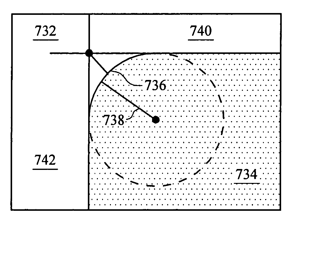
A corner formed of orthogonally intersecting lines in a mask pattern frequently produces an undesirably rounded structure when transferred to the device layer due to the proximity effect which causes light to scatter from the proximate orthogonal edges of the mask pattern.
This technique is not available to compensate for the proximity effect when substantially orthogonal lines intersect and the proximity effect increases toward the intersection.

Method used


Image

  • Utilizing compensation features in photolithography for semiconductor device fabrication
  • Utilizing compensation features in photolithography for semiconductor device fabrication
  • Utilizing compensation features in photolithography for semiconductor device fabrication

Examples


Embodiment Construction

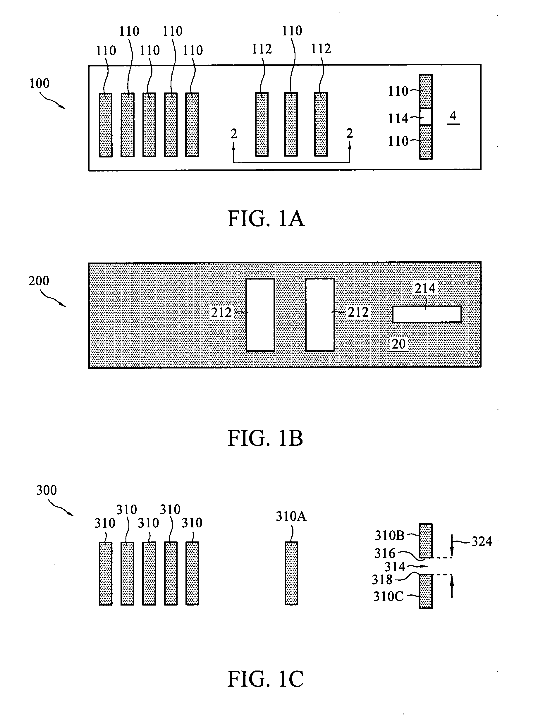
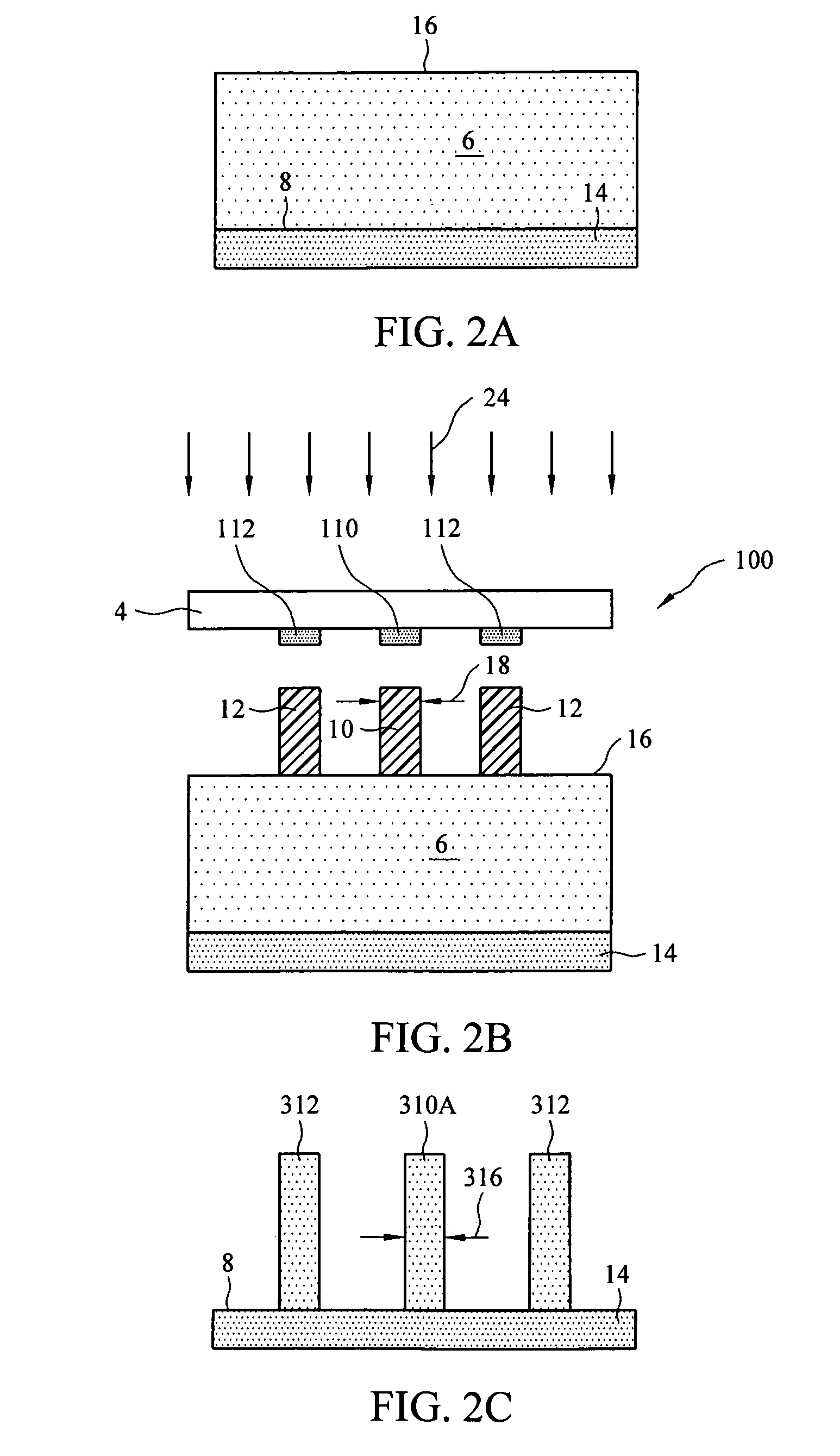
[0024] One aspect of the present invention overcomes the limitations of the prior art and provides compensation features such as scattering bars added to a photomask pattern. The compensation features are patterned and etched along with device features, then removed. They may be removed by patterning using a second mask of a set used on a single device level. The compensation features may be used at any of various mask levels and in conjunction with the production of various semiconductor devices. In one embodiment, the compensation features may be scattering bars used in conjunction with an isolated line or an outermost line of an array of lines. The compensation feature is sufficiently wide to improve the depth of focus for isolated or outermost lines of the desired pattern which are situated differently than otherwise similar nested lines. In an another embodiment, the compensation feature may be a line segment connecting two linearly aligned device features. When this exemplary ...


PUM

PropertyMeasurementUnit
widthaaaaaaaaaa
widthaaaaaaaaaa
distanceaaaaaaaaaa

Abstract

A photomask set includes at least two masks that combine to form a device pattern in a semiconductor device. Orthogonal corners may be produced in a semiconductor device pattern to include one edge defined by a first mask and an orthogonal edge defined by a second mask. The mask set may include a first mask with compensation features and a second mask with void areas overlaying the compensation features when the first and second masks are aligned with one another, such that the compensation features are removed when patterns are successfully formed from the first and second masks. The compensation features alleviate proximity effects during the formation of device features.

Description

RELATED APPLICATION [0001] This application is a continuation-in-part of pending U.S. patent application Ser. No. 10 / 842,065, filed May 10, 2004.FIELD OF THE INVENTION [0002] The present invention relates most generally, to photolithography and etch processes in semiconductor device manufacturing. More particularly, the present invention relates to a photomask system for decreasing the proximity effect and improving the definition of device features. BACKGROUND [0003] In today's rapidly advancing semiconductor manufacturing industry, the demand for increasing levels of device integration requires that device features are made increasingly smaller and in closer proximity to one another. The most critical steps in defining and ultimately producing device features are the photolithography and etching operations. As such, higher levels of device integration will likely be enabled by technological advances in the photolithography and / or etch processes. In order to meet this demand, proce...

Claims


Application Information

Patent Timeline
Patent Type & Authority Applications(United States)
IPC IPC(8): G03C5/00G03F1/14G03F9/00H01L21/469
CPCG03F1/36G03F1/144G03F1/70
Inventor CHEN, KUEI SHUNLIN, CHIN-HSIANGCHIU, CHIH-CHENG
Owner TAIWAN SEMICON MFG CO LTD
Learn More