
Manufacturing method for semiconductor device and semiconductor manufacturing apparatus

Inactive Publication Date: 2005-10-20
RENESAS TECH CORP
View PDF8 Cites 2 Cited by
  • Summary
  • Abstract
  • Description
  • Claims
  • Application Information

AI Technical Summary

Benefits of technology

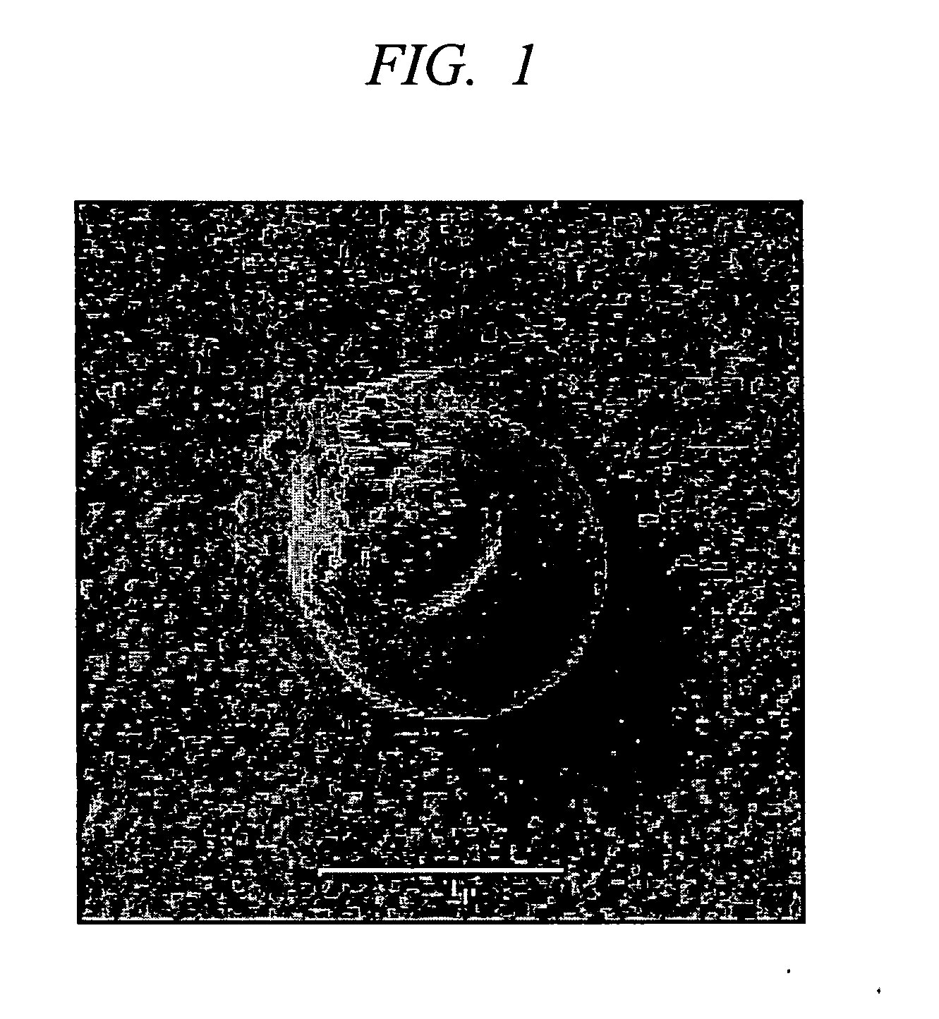
[0011] As a result of various examinations of a difference between the batch processing and the single-wafer processing the inventors of the present invention have found the fact as follows. That is, in the usual batch processing, the polycrystalline silicon film is formed on a large number of wafers at a time by the low pressure CVD or the like, and then the wafers are transferred into the air while being maintained in a high temperature. Therefore, the polycrystalline silicon on the wafer naturally reacts with oxygen in the air and an oxide film is formed thereon, and the naturally formed oxide film suppresses the abnormal growth of the polycrystalline silicon.
[0015] If the line of the single-wafer processing is properly operated, the abnormal growth of the polycrystalline silicon does not cause any problem. However, there is much possibility that the line is stopped for six hours or more due to the trouble of apparatus. If the abnormal growth of polycrystalline silicon formed on the wafer occurs in every line stop and the like, the percent of product defect becomes extremely high and the throughput is significantly reduced, which greatly influences the production efficiency.
[0016] Also, the above-described abnormal growth of polycrystalline silicon occurs also in an event other than the transition to the next step. For example, even in the case where the polycrystalline silicon is patterned in the latter step, there is a strong possibility that the abnormal growth will occur during the time when the surface of the polycrystalline silicon is exposed to the surrounding atmosphere. A fluorine-based gas such as SF6 is used in the patterning of the polycrystalline silicon. However, if the polycrystalline silicon having the fluorine-based gas left on the surface thereof is exposed to the air, the abnormal growth easily occurs even in a short time.
[0018] An object of the present invention is to suppress the occurrence of film surface abnormality, for example, an abnormal growth on a silicon film formed on a wafer.
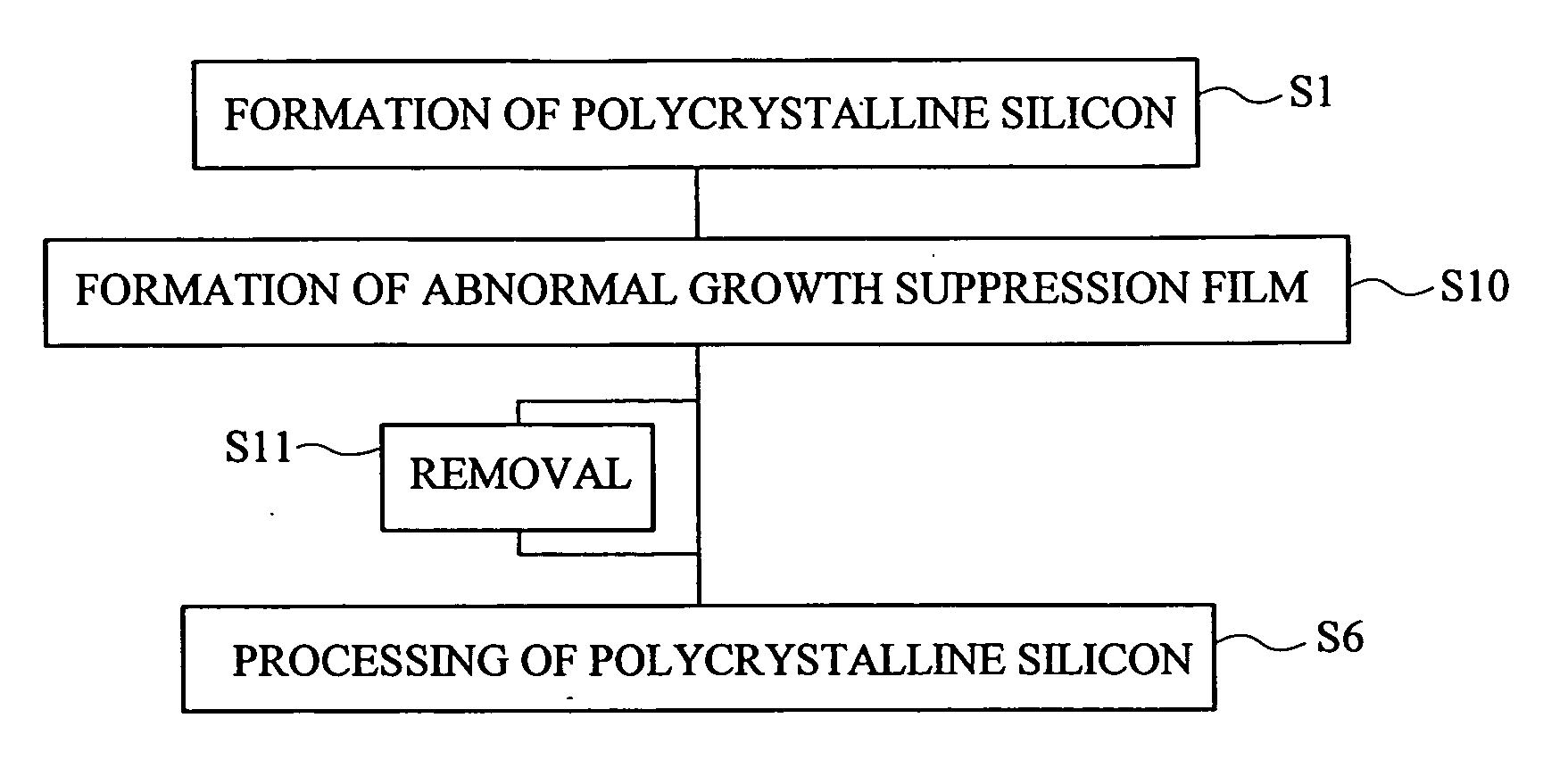
[0021] More specifically, in the present invention, after forming a silicon film, an oxide film is formed on the surface within a predetermined time or the next process is executed within a predetermined time so as to prevent the occurrence of the abnormal growth on the film surface. The surface of the polycrystalline silicon or amorphous silicon is forcibly oxidized by using oxidation means such as ozone water immediately after forming the polycrystalline silicon or amorphous silicon on the wafer without relying on the natural oxidation. By doing so, the surface abnormality of a film can be suppressed.
[0023] According to the present invention, even in the single-wafer processing different from the batch processing, the abnormal growth of polycrystalline silicon or amorphous silicon formed on the wafer can be suppressed.

Problems solved by technology

However, when the line is stopped for the regular cleaning of a clean room or the like, the wafers on which the polycrystalline silicon is formed are left in a standby state in the FOUP for a long time and, in such a standby state, the abnormal growth occurs on the polycrystalline silicon formed on the wafers.

Method used


Image

  • Manufacturing method for semiconductor device and semiconductor manufacturing apparatus
  • Manufacturing method for semiconductor device and semiconductor manufacturing apparatus
  • Manufacturing method for semiconductor device and semiconductor manufacturing apparatus

Examples


first embodiment

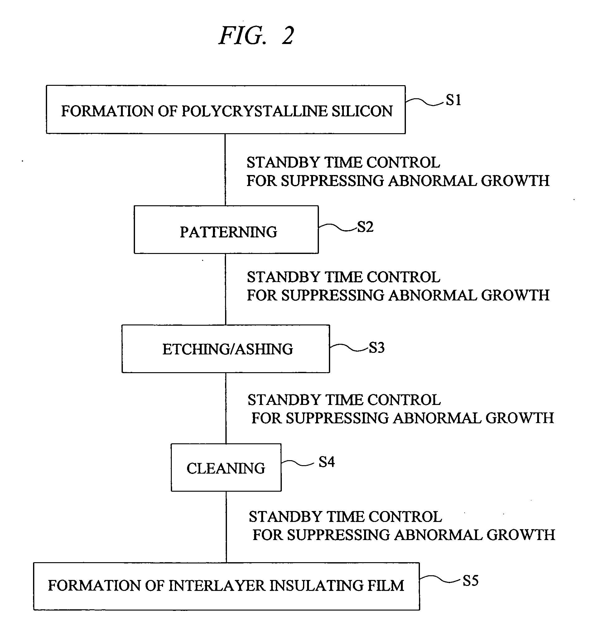
[0038] For the suppression of the abnormal growth on a surface of a polycrystalline silicon film formed on a wafer, a manufacturing method of a semiconductor device according to the present invention will be described in this embodiment in which a standby time is controlled so as to minimize the occurrence of the abnormal growth in the single-wafer processing of polycrystalline silicon as shown in FIG. 2.

[0039] More specifically, in the process shown in FIG. 2, a polycrystalline silicon film is formed on a wafer by CVD in step S1. In step S2, the formed polycrystalline silicon film is patterned. For example, a photosensitive resist is formed on the polycrystalline silicon, the resist is exposed using a predetermined pattern and then is developed to form an etching mask, and the polycrystalline silicon is patterned by the etching using a fluorine-based gas etc. along the etching mask.

[0040] In step S3, the etching mask is removed by the etching using the fluorine-based gas and then...

second embodiment

[0045] In a second embodiment, the case where a manufacturing method for a semiconductor device according to the present invention is applied to the suppression of the abnormal growth of polycrystalline silicon formed on the wafer will be described.

[0046] In the first embodiment, the method of preventing the abnormal growth of silicon by controlling the standby time of each step, that is, by setting the standby time to be short enough to prevent the occurrence of the abnormal growth on a film surface has been described. However, depending on on-site conditions, the time control as described above is sometimes difficult. Furthermore, when any of the steps is stopped due to the line trouble or the like, the predetermined standby time may be extended and the time control as planned cannot be performed in some cases.

[0047] Therefore, as a method for suppressing the surface abnormality of silicon other than the above-described method of controlling the standby time, in which the next p...

third embodiment

[0094] In a third embodiment, based on the manufacturing method of a semiconductor device described in the second embodiment, the semiconductor manufacturing apparatus capable of forming the abnormal growth suppression film with the same effects as described in the second embodiment by using the gas functioning as the oxidizing agent instead of the liquid oxidizing agent such as the ozone water and the hydrogen peroxide solution will be described.

[0095]FIG. 8 is an explanatory diagram schematically showing the semiconductor manufacturing apparatus 30 according to the present invention represented by the CVD apparatus (Chemical Vapor Deposition apparatus) 30a used as the multi-chamber polycrystalline silicon forming apparatus.

[0096] As shown in FIG. 8, the CVD apparatus 30a is provided with a load port 31 at which the wafer is transferred from the previous step and to the next step. A plurality of wafers are collectively stored in a wafer storing unit such as a FOUP and, in this st...


PUM

PropertyMeasurementUnit
Thicknessaaaaaaaaaa
Surfaceaaaaaaaaaa

Abstract

The present invention provides a technology for suppressing occurrence of abnormality on a surface of a silicon film other than a single crystal film formed on a wafer. A silicon film is formed on a wafer in step S1 and an oxide film functioning as an abnormality suppression film for suppressing the surface abnormality is formed on the silicon surface on the wafer formed in step S10. The abnormality suppression film is formed by the surface oxidation of the polycrystalline silicon using chemical solution such as ozone water or hydrogen peroxide solution. After forming the abnormality suppression film on the silicon surface, the abnormality suppression film, for example, an abnormal growth suppression film is removed according to need, and then the process of patterning the silicon film and forming an insulating oxide film is performed.

Description

CROSS-REFERENCE TO RELATED APPLICATION [0001] The present application claims priority from Japanese Patent Application JP 2004-124677 filed on Apr. 20, 2004, the content of which is hereby incorporated by reference into this application. TECHNICAL FIELD OF THE INVENTION [0002] The present invention relates to a technology for suppressing an abnormal growth on a surface of a silicon film other than a single crystal film used for a semiconductor device, that is, an abnormal growth of silicon on a surface of a polycrystalline silicon film and an amorphous silicon film. More particularly, it relates to a technology effectively applied to a single-wafer processing including a step of forming a polycrystalline silicon film. BACKGROUND OF THE INVENTION [0003] The technology described below has been examined during the development of the present invention by the inventors thereof, and its outline will be shown as follows. [0004] In a manufacturing process of the semiconductor device, a sili...

Claims


Application Information

Patent Timeline
IPC IPC(8): H01L21/31H01L21/20H01L21/28H01L21/316H01L21/336H01L21/8247H01L21/84H01L27/115H01L27/12H01L29/423H01L29/78H01L29/786H01L29/788H01L29/792
CPCH01L21/28035H01L21/3165H01L29/42324H01L27/12H01L21/84H01L21/02164H01L21/02282H01L21/02238H01L21/02307H01L21/02554H01L21/32105
Inventor TSUGA, TOSHIHITOYAMAMOTO, HIROHIKOFUNABASHI, MICHIMASANEMOTO, KAZUNORI
Owner RENESAS TECH CORP
Learn More