
Method and device for high sensitivity detection of the presence of dna and other probes

a technology applied in the field of high sensitivity detection of the presence of dna and other probes, can solve the problems of limited external optical detection of a specific opaque label such as silver, long processing time, and possibility of false positive readings

Inactive Publication Date: 2005-10-13
UNIVERSITE CATHOLIQUE DE LOUVAIN
View PDF17 Cites 88 Cited by
  • Summary
  • Abstract
  • Description
  • Claims
  • Application Information

AI Technical Summary

Benefits of technology

[0010] It is an object of the present invention to provide a method and a device for measuring the presence of target molecules or materials, especially target biological molecules and materials, as fast as possible, and preferably as soon as a very low amount of the target molecule or material is present.
[0013] It is yet another object of the present invention to limit the time required for measuring the presence of target molecules or materials, especially target biological molecules and materials, and hence improve the usefulness or to reduce cost.

Problems solved by technology

The external optical detection of a specific opaque label such a silver is limited by the resolution of low cost scanners: the spots must be larger than 100 μm.
However, precipitation of silver is also initiated by the bare gold electrodes, so when the bridge finally has been formed, it is not sure whether this is because silver has been precipitated on one or a plurality of gold nanoballs, or whether just a short-circuit between the electrodes has been formed by silver precipitation on the electrodes.
These processes lead to the possibility of false positive readings.
With this known technique, processing time is quite long, quantitative detection can be imprecise and a calibration prior to measurement is impossible, that is it is not possible to calibrate to a definite positive result level.
The resistance, therefore, decreases by several orders of magnitude to a value whose absolute value is difficult to interpret making hybridised DNA quantification, difficult.
This may provide a good signal to noise ration for an indication of hybridisation, but deriving further information from the shape of the curve or from the absolute resistance values is difficult.
However, these materials are hardly compatible with conventional integrated circuit fabrication.
A number of barriers need to be provided between the metal and the semiconductor material on which the detector is fabricated, in order to avoid that the metal diffuses into the semiconductor material, thus leading to contamination and degradation of the active devices in the semiconductor circuits.
Furthermore, the processing of the semiconductor chip and the application of the noble metal has to be done in separate clean rooms (to avoid cross-contamination between processes), which makes the fabrication of such detector chips more complex and expensive.
Also, a major limitation related to the use of hybridised DNA alone (no labels or markers to assist) concerns the sensitivity since the methods can generally only detect a change of a factor of 100% at the maximum, between single strand DNA probe (in case of no hybridisation) or hybridised DNA (i.e. two strands only instead of one).
The detection of permittivity changes between two electrodes due to DNA binding alone is also limited by the sensitivity, which is hardly more than a few tens of percents.

Method used


Image

  • Method and device for high sensitivity detection of the presence of dna and other probes
  • Method and device for high sensitivity detection of the presence of dna and other probes
  • Method and device for high sensitivity detection of the presence of dna and other probes

Examples


example

Materials and Processes

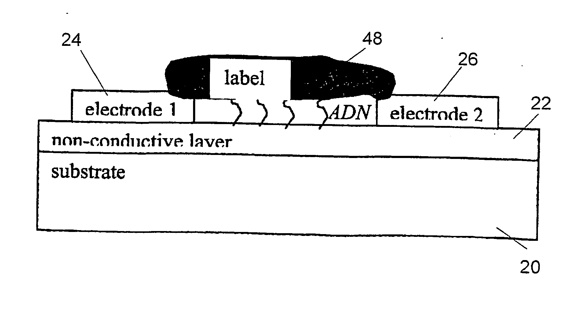
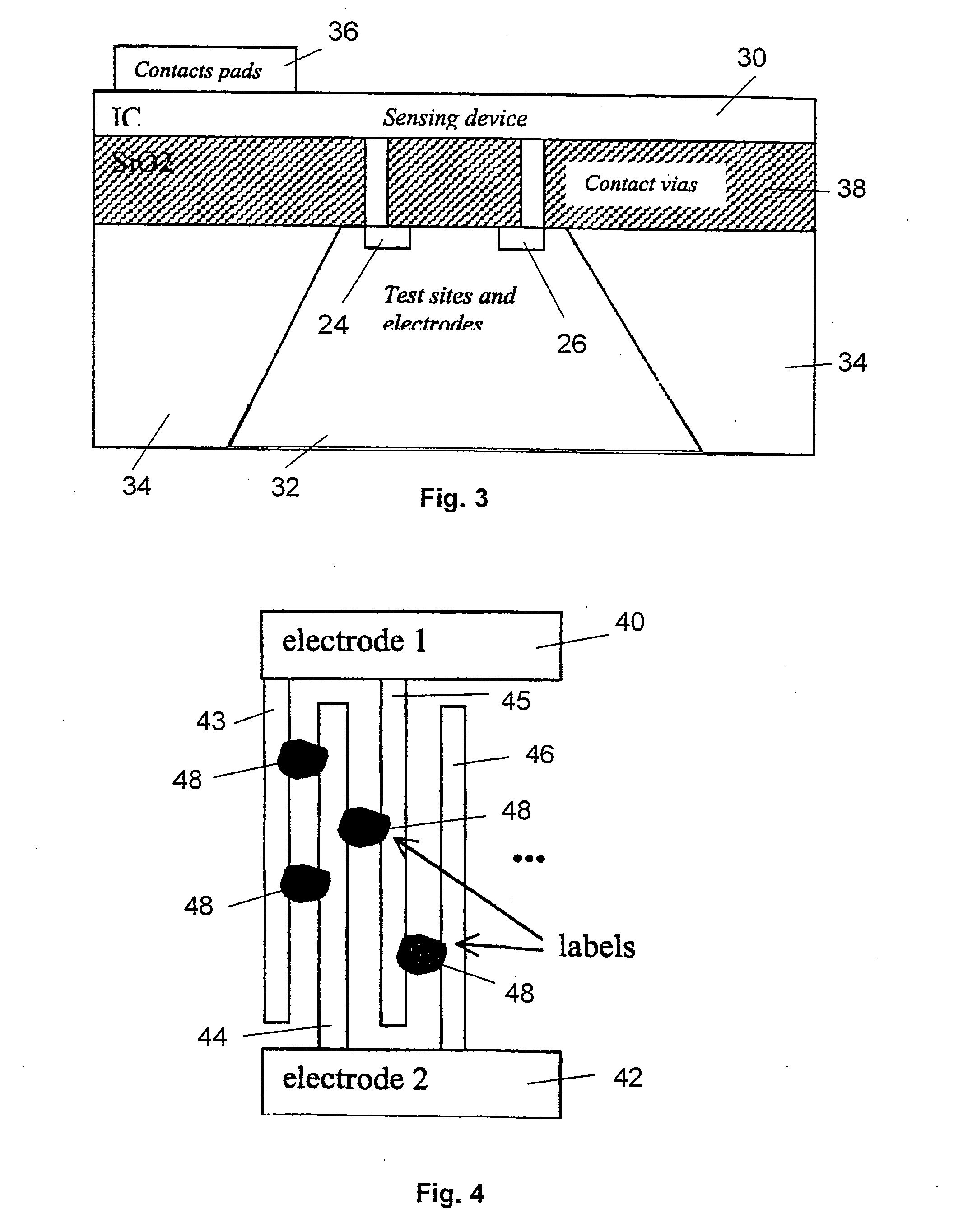
[0109] Standard P-doped Si wafers were used to make the chips according to the present invention. In order to insulate the electrodes from the substrate and lowering the parasitic bulk effects, a 400 nm thick thermal wet oxide (SiO2) was grown—in fact previous experiments showed that this kind of material enhanced the binding of DNA to the support. The growing temperature and time of the SiO2 were 1000° C. and 1 h 16 min respectively. To guaranty a pure wet oxide, a short delay of around 1 minute only was left between oxygen and hydrogen valves opening.

[0110] The electrodes were manufactured with pure aluminium, by means of a lift-off process. This was preferred to an etching method because previous tests used to show a non-specific silver precipitation on a 240 nm-thick silicon oxide in the second case, after deposition and plasma etch of 1 μm of {Al+2% Si}. In the lift-off process, an aluminium thickness of 500 nm was used, and nitric acid was used for th...


PUM

PropertyMeasurementUnit
Distanceaaaaaaaaaa
Distanceaaaaaaaaaa
Sizeaaaaaaaaaa

Abstract

The present invention provides a method for capacitive detection of the presence of target sample on a substrate, which comprises the steps of: binding a target sample to selective binding sites on the substrate, the target sample being directly or indirectly labeled with conductive labels, and sensing the presence of the bound conductive labels to a binding site to thereby determine the presence of the target sample. The sensing step is carried out by a capacitive detection of the presence of the conductive labels. The present invention also provides a capacitive sensor device for determining the presence of a target sample. Conductive labels are directly or indirectly couplable to the target sample. The capacitive sensor device comprises a substrate having attached thereto a binding site able to selectively bind a target sample, a capacitive sensor element, and sensing circuitry for determining the presence of a target sample bound to the binding site by application of electrical signals to a capacitive sensor element. The capacitive sensor element comprises a set of at least two electrodes with non-conductive surfaces in a region associated with the binding site.

Description

TECHNICAL FIELD OF THE INVENTION [0001] The present invention relates to a method and apparatus for sensing of the presence of a molecular species or substance bound to a binding site, especially by means of conductive labels. In particular it relates to apparatus and methods for capacitive detection of binding of biological molecules on a micro-array or biochip. BACKGROUND OF THE INVENTION [0002] The introduction of micro-arrays or biochips is revolutionising the analysis of DNA (desoxyribonucleic acid), RNA (ribonucleic acid), proteins, other molecules, e.g. herbicides and pesticides, or other micro- or nanomaterials, e.g. microcarriers such as beads. Applications are, for example, human genotyping (e.g. in hospitals or by individual doctors or nurses), bacteriological screening, biological and pharmacological research. [0003] Biochips, also called biosensor chips, biological microchips, gene-chips or DNA chips, consist in their simplest form of a substrate on which a large number...

Claims


Application Information

Patent Timeline
IPC IPC(8): C12Q1/68G01N27/02G01N27/22G01N33/543
CPCG01N27/221G01N27/226Y10T436/163333Y10T436/173845Y10T436/147777G01N33/5438
Inventor FLANDRE, DENISMORENO, LUISPAMPIN, REMIBOURGEOIS, DAVIDREMACLE, JOSELOBERT, PIERRE-EMMANNUEL
Owner UNIVERSITE CATHOLIQUE DE LOUVAIN
Learn More