
Binary frequency-shift keying demodulator and frequency-to-voltage converter

a demodulator and frequency-to-voltage converter technology, applied in the field of wireless communication receiver devices, can solve the problems of power consumption, special difficulty in implementation, and the addition of an external phase-shifting circuit, etc., and achieve the effects of reducing power consumption rate, simple circuit board design, and reducing charge injection

Active Publication Date: 2005-10-13
SPREADTRUM COMM (SHANGHAI) CO LTD
View PDF2 Cites 12 Cited by
  • Summary
  • Abstract
  • Description
  • Claims
  • Application Information

AI Technical Summary

Benefits of technology

[0006] The present invention is to provide a BFSK demodulator that is without external support and has a simpler but more condensed circuit structure design. For lowering Bit-Error Rate (BER), the present invention also provides a frequency-to-voltage circuit.
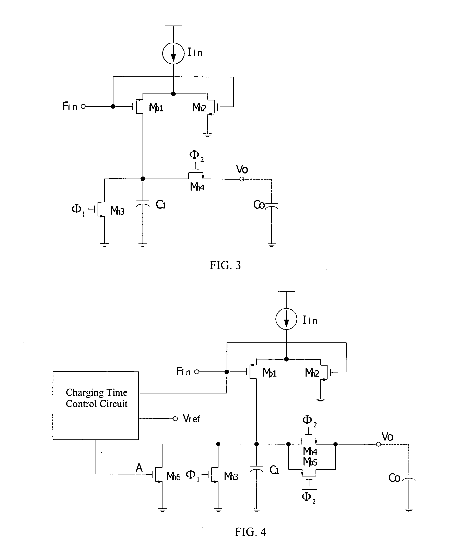
[0010] The present invention provides a BFSK demodulator further comprising a PMOS transistor Mp5, a NMOS transistor Mn6, and a charge time control circuit. Transistor Mp5 is implemented to reduce the charge injection effect. The source terminal of the Mp5 is connected with the drain terminal of Mn4, while the drain terminal of Mp5 is connected to the source terminal of Mn4. The gate terminal of Mp5 is connected to signal φ2. The drain terminal of transistor Mn6 is connected with the drain terminal of transistor Mp5, where as the source terminal is connected to the ground. The time control circuit is connected ill between the input signal Fin and the gate terminal of transistor Mn6, and controls the C1 charging time from current source Iin bypassing the transistor Mn6.
[0011] The present invention does not require any external support elements. The present invention has a simpler, smaller circuit board design, and has a lower power consumption rate.
[0012] Comparing to existing differential demodulator, the present invention abandoned the low-pass filter, adopted a comparatively simpler comparator circuit using a referenced voltage. Since the referenced voltage signal and the information voltage input signal are produced by the same frequency-to-voltage converter, the sensitivities toward the fabrication environments also appear to be similar. Also, the time controlled frequency-to-voltage-converter circuit can efficiently enlarge the voltage difference matching the demodulated frequencies, and improve the Bit-Error Rate.
[0013] Thus, present invention has the advantage of employing a simpler, smaller, but more condensed circuit implementation, having a better Bit-Error rate.

Problems solved by technology

However, this implementation is especially difficult in dealing with functional dispersedness caused by external implemented elements.
The major disadvantages of differential demodulator are the lager circuit board design, which causes power consumption, and a necessary addition of an external phase-shifting circuit.
Therefore under the circumstances when the information signal is similar to carrier signal, the demand on the filter is higher, such a differential demodulator is not appropriate anymore.

Method used


Image

  • Binary frequency-shift keying demodulator and frequency-to-voltage converter
  • Binary frequency-shift keying demodulator and frequency-to-voltage converter
  • Binary frequency-shift keying demodulator and frequency-to-voltage converter

Examples


Embodiment Construction

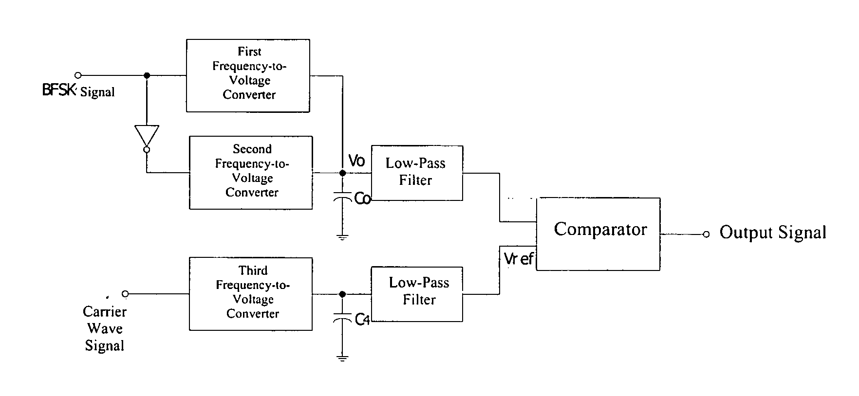
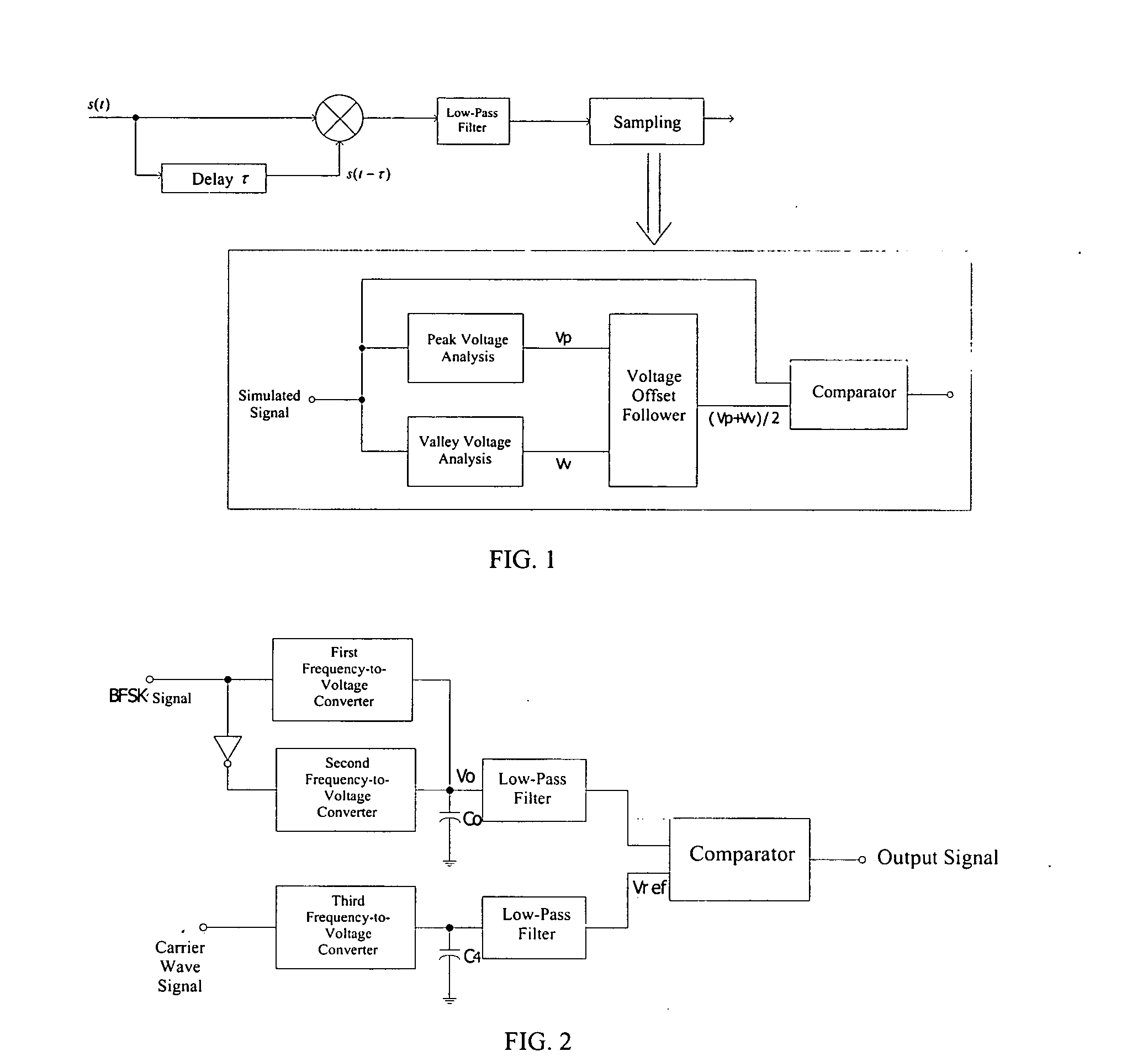
[0019] As is seen in FIG. 2, the present invention provides a BFSK demodulator comprising a three-channel frequency-to-voltage converter. Frequency-to-voltage converter converts a frequency signal into a voltage signal. A BFSK information signal is input into the first-channel frequency-to-voltage converter and a converted BFSK information signal is input the second-channel frequency-to-voltage converter. The outputs of first and second channel frequency-to-voltage converter are connected with a capacitor Co, whereas the other end of the capacitor Co is connected to the ground. A voltage signal Vo is produced by the first and second frequency-to-voltage converters and the capacitor. The voltage signal Vo becomes the positive input to the comparator after high frequency noise filtering through a first low-pass filter. Converting the BFSK information signal and using the same frequency-to-voltage circuits are to rearrange electron more frequent. Therefore charges are conducted on capa...


PUM


Abstract

A BFSK demodulator comprises a three-channel frequency-to-voltage converter, an information signal inputting the first-channel frequency-to-voltage converter, a converted information signal inputting the second-channel frequency-to-voltage converter, wherein outputs of first and second channel frequency-to-voltage converter are connected with a capacitor, a output voltage signal produced by the first and second frequency-to-voltage converters and the capacitor, inputting into a positive terminal of the comparator after high frequency noise filtering through a first low-pass filter, a carrier signal inputs into the third-channel frequency-to-voltage converter; and an output from the third-channel frequency-to-voltage converter connected to a capacitor; and a reference voltage signal is produced after high frequency noise filtering through a second low-pass filter, producing a demodulated signal after comparing the information voltage signal with the reference voltage.

Description

TECHNICAL FIELD [0001] The present invention relates to a wireless communication receiver device, particularly relates to a binary frequency-shift keying demodulator comprising a frequency-to-voltage converter. BACKGOUND OF THE INVENTION [0002] Among wireless communication devises, demodulator is often seen as one of the most important component in receiver end. Demodulators are utilized at the rear end of the receiver to demodulate the signal modulated from the front end, matching the initial information signal. Bit Error-Rate (BER) is the important key to rate such demodulators. Current Binary Frequency-Shift Keying (BFSK) signal demodulation methods can be categorized as coherent demodulation and incoherent demodulation, where the incoherent demodulation has lower resistance to noise. Among several coherent demodulation implementations, differential demodulator is easily structured and it also provides lower Bit Error-Rate. In addition, differential demodulator does not require l...

Claims


Application Information

Patent Timeline
Patent Type & Authority Applications(United States)
IPC IPC(8): H02M3/24H04L27/06H04L27/14
CPCH04L27/06
Inventor LI, LARRY B.ZHANG, ZHAOFENGWU, JUN
Owner SPREADTRUM COMM (SHANGHAI) CO LTD
Learn More