
Low-resistance n type semiconductor diamond and process for producing the same

Inactive Publication Date: 2005-10-06
SUMITOMO ELECTRIC IND LTD
View PDF6 Cites 3 Cited by
  • Summary
  • Abstract
  • Description
  • Claims
  • Application Information

AI Technical Summary

Benefits of technology

[0012] The present invention has been brought about to address the issues noted above. In particular, an object of the present invention is to solve the problems that arise in lithium-doping situations, to afford low-resistivity n-type semiconductor diamond of excellent crystal quality, and a method of manufacturing the diamond.

Problems solved by technology

Moreover, given that the dependence of the resistivity of these n-type semiconductor diamonds on temperature is considerable because their activation energy is extraordinarily large—for the phosphorous-doped diamond it is approximately 0.6 eV, and for the sulfur-doped it is approximately 0.4 eV—across a wide temperature range, stable application of devices employing these n-type semiconductor diamonds has been problematic.
Inasmuch as the covalent radii of phosphorous and sulfur are appreciably large compared with the covalent radius of carbon, a problem in situations in which vapor synthesis is carried out while doping with phosphorous and sulfur has been that if diamond is vapor-deposited to a thickness on the order of 10 μm or more, cracks appear in the deposited diamond.
Nonetheless, problems with these methods have been that stable electrical properties cannot be achieved because the lithium moves around within the diamond, and that during the vapor deposition of diamond, what with the lithium bonding with hydrogen that is incorporated at the same time, the lithium is not electrically activated.
A large amount of lithium and nitrogen ends up being doped into the diamond lattice interstices, yet with this method the density at which the lithium and nitrogen are incorporated is not readily controlled.
A further problem with the nitrogen has been that though it is doped into the lattice interstices, it does not become activated as an n-type dopant at all; the nitrogen doped in large quantity in the lattice interstices drastically deteriorates the n-type semiconductor characteristics such that the low-resistivity n-type semiconductor properties sought cannot be achieved.

Method used


Image

  • Low-resistance n type semiconductor diamond and process for producing the same
  • Low-resistance n type semiconductor diamond and process for producing the same

Examples


embodiment

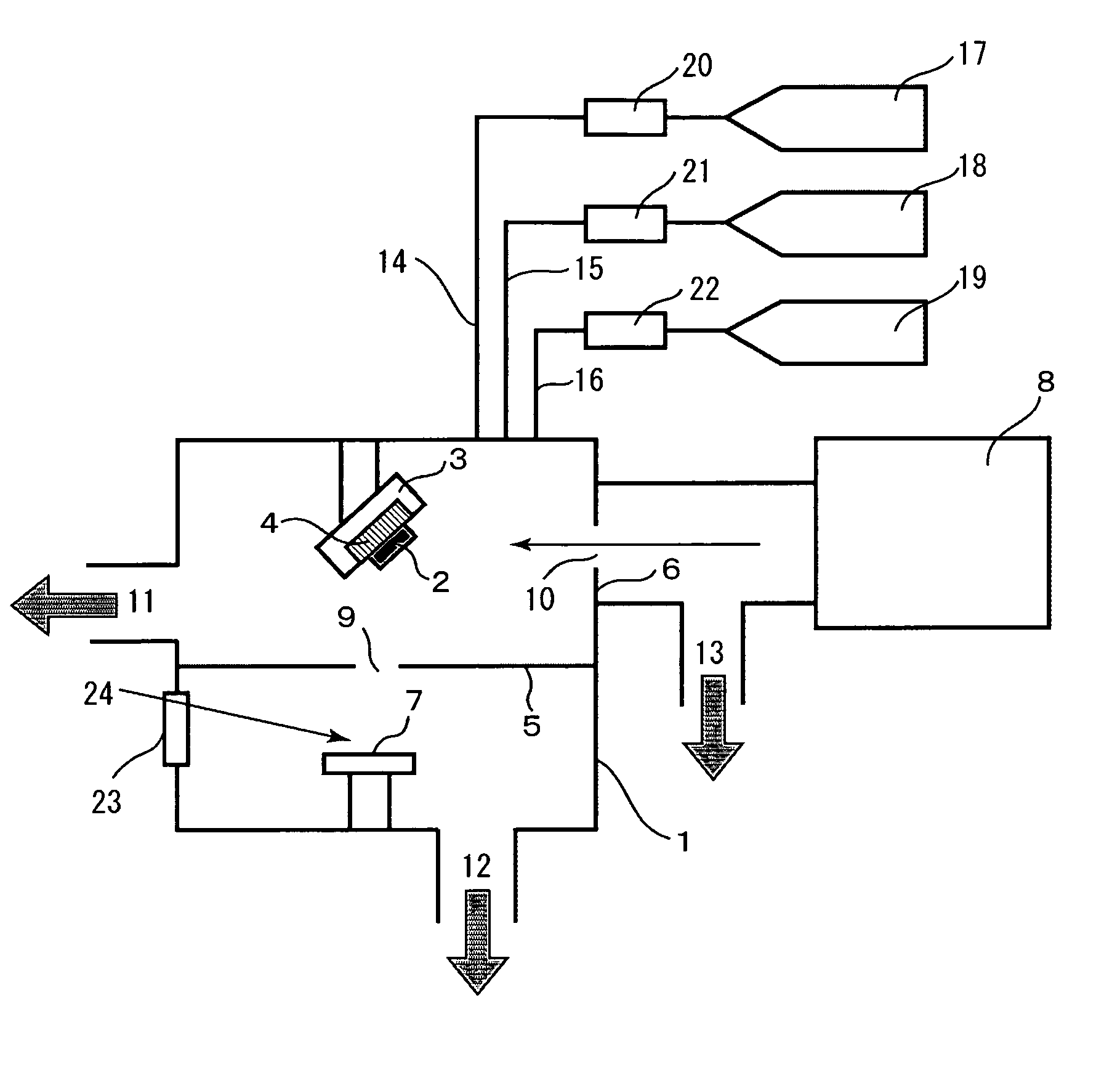
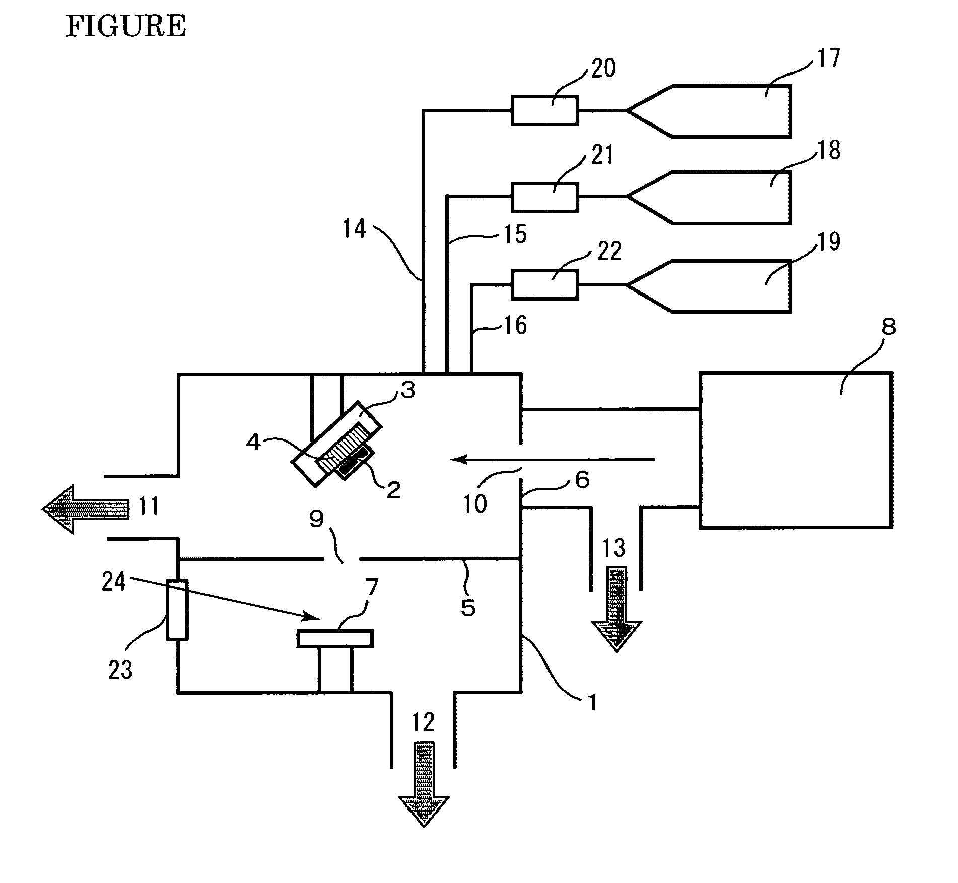
[0029] The FIGURE is a schematic diagram illustrating one example of a diamond-synthesizing apparatus utilized in an embodiment of the present invention.

[0030] A diamond substrate 2 is set into a substrate holder 3 within a vacuum chamber 1. The temperature of the diamond substrate 2 can be adjusted by a heating device 4 from room temperature to a temperature of a thousand several hundred degrees. The vacuum chamber 1 is divided by pressure-differential partitions 5 and 6 into a section containing the diamond substrate 2, a section containing a target 7 consisting of lithium oxide, and a section to which a light source 8 is connected. Slits 9 and 10 are provided in the respective pressure-differentiating partitions, and the sections just described are furnished with respective separate vacuum-evacuation ports 11, 12 and 13 in order for pressure-differential evacuation to take place through them. The section containing the diamond substrate 2 is furnished with gas introduction lines...


PUM

PropertyMeasurementUnit
Temperatureaaaaaaaaaa
Pressureaaaaaaaaaa

Abstract

Concerns lithium-doped diamond: Low-resistivity n-type semiconductor diamond doped with lithium and nitrogen, and a method of manufacturing such diamond are provided. Low-resistivity n-type semiconductor diamond containing 1017 cm−3 or more of lithium atoms and nitrogen atoms together, in which are respectively doped lithium atoms into carbon-atom interstitial lattice sites, and nitrogen atoms into carbon-atom substitutional sites, with the lithium and the nitrogen holding arrangements that neighbor each other. To obtain low-resistivity n-type semiconductor diamond, in a method for the vapor synthesis of diamond, photodissociating source materials by photoexcitation utilizing vacuum ultraviolet light and irradiating a lithium source material with an excimer laser to scatter and supply lithium atoms enables the diamond to be produced.

Description

TECHNICAL FIELD [0001] The present invention relates to low-resistivity n-type semiconductor diamond doped with both lithium and nitrogen, and to methods of manufacturing such diamond. More particularly lithium atoms are doped into carbon-atom interstitial lattice sites in single-crystal diamond, and nitrogen atoms into carbon-atom substitutional sites therein, with the dopants holding neighboring arrangements. The present invention then relates to a method of manufacturing by vapor synthesis the inventive low-resistivity n-type semiconductor diamond—by vapor synthesis that relies on photo-dissociating the precursor using vacuum ultraviolet light. BACKGROUND ART [0002] Diamond has been employed as a semiconductor material for some time, and research into its practical application as a basis for semiconductor devices is ongoing. [0003] In diamond, with its extraordinarily large bandgap of 5.5 eV, no intrinsic gap—in which carrier conduction is forbidden—as a semiconductor exists at t...

Claims


Application Information

Patent Timeline
IPC IPC(8): C30B29/04C23C16/27C23C16/448C23C16/48C30B25/10H01L21/205H01L21/22
CPCC23C16/27C23C16/278C23C16/448C23C16/482C30B25/105H01L21/02376H01L21/02634H01L21/02527H01L21/02576H01L21/0262C30B29/04
Inventor NAMBA, AKIHIKOIMAI, TAKAHIROTAKEUCHI, HISAO
Owner SUMITOMO ELECTRIC IND LTD
Learn More