Thin-film semiconductor device and method of manufacturing the same
a technology of thin film and semiconductor, applied in semiconductor devices, semiconductor/solid-state device details, electrical devices, etc., can solve the problems of ineffective use of limited resources, most parts are ground and wasted, and the normal semiconductor chip itself has no flexibility, so as to achieve efficient separation independent of the wafer area
- Summary
- Abstract
- Description
- Claims
- Application Information
AI Technical Summary
Benefits of technology
Problems solved by technology
Method used
Image
Examples
first embodiment
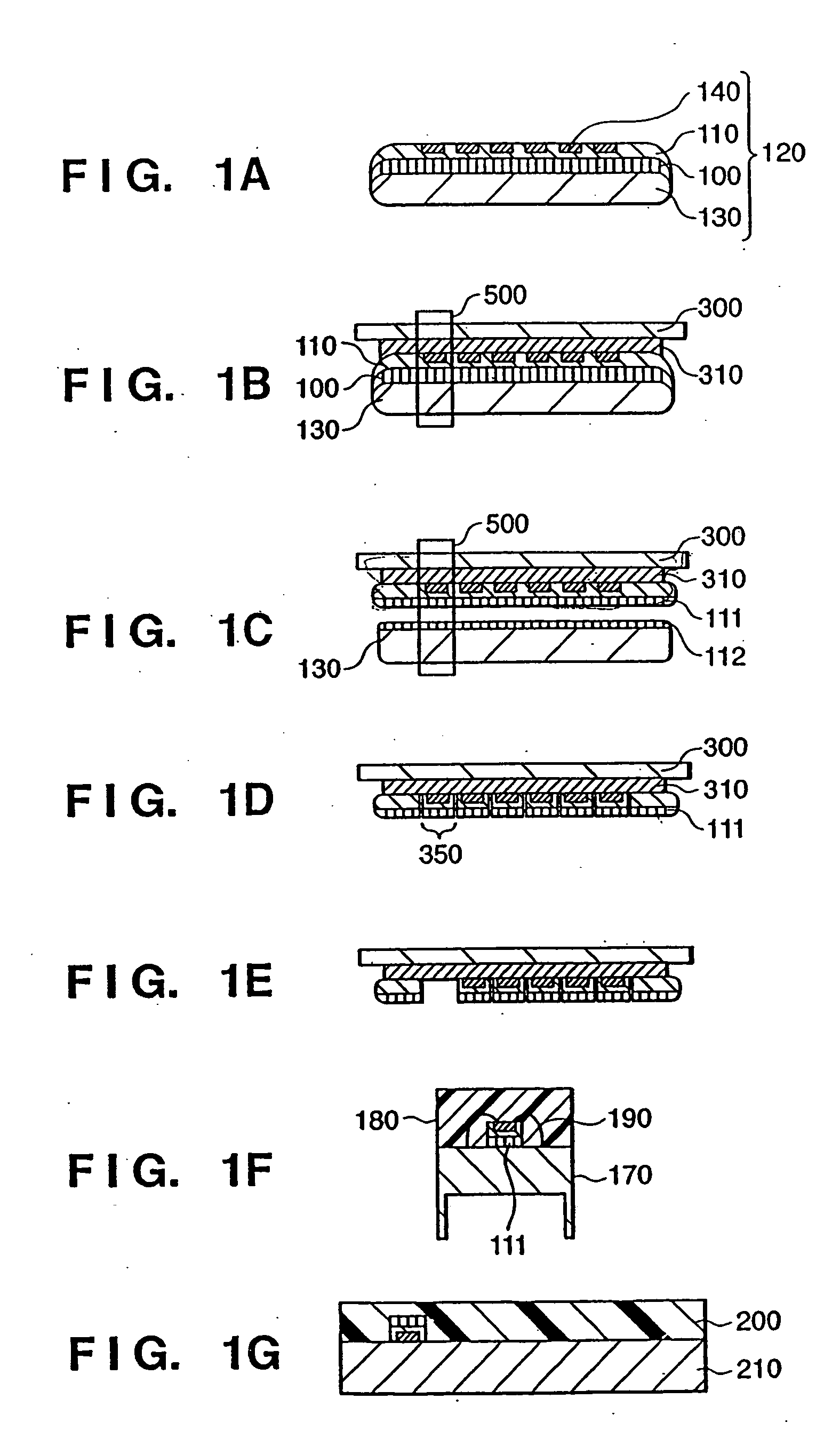
[0028] The first embodiment of the present invention will be described with reference to FIGS. 1A to 1G.
[0029] First, as shown in FIG. 1A, a member 120 having a semiconductor film 110 with semiconductor elements and / or semiconductor integrated circuits 140 on a semiconductor region 130 via a separation layer 100 is prepared. A method of forming the semiconductor elements and / or semiconductor integrated circuits 140 on the semiconductor film 110 will be described later.
[0030] The member 120 is separated at the separation layer 100. More specifically, a pressure by a fluid is applied to the side surface of the separation layer 100. To apply a pressure, preferably, a fluid formed from a liquid or gas is injected to the side surface of the separation layer 100 as high-pressure jet, or a static pressure is applied to the separation layer 100.
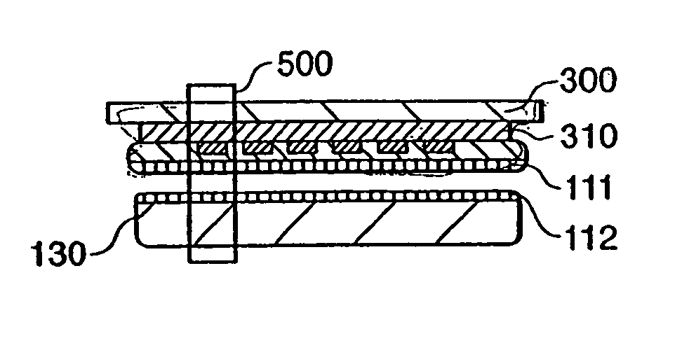
[0031] In separation, the member 120 may be bonded to a support member 300 via an adhesive layer 310 (FIG. 1B). The step of bonding the member to...
second embodiment
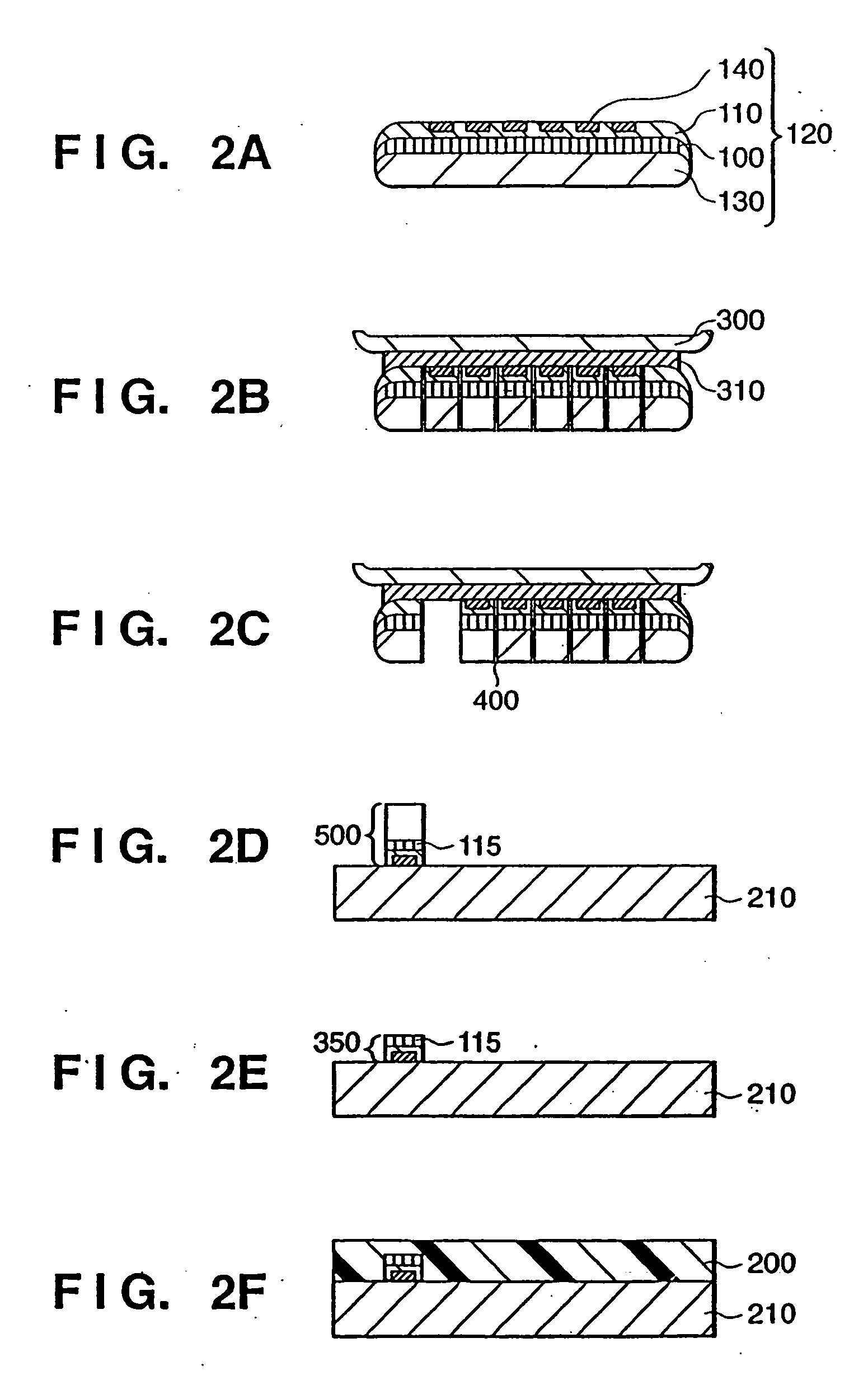
[0058] The second embodiment of the present invention will be described next with reference to FIGS. 2A to 2F.
[0059] As in the first embodiment, a member 120 having a semiconductor film 110 with semiconductor elements and / or semiconductor integrated circuits 140 on a semiconductor region 130 via a separation layer 100 is prepared. (FIG. 2A).
[0060] The member 120 is bonded to a support member 300 via an adhesive layer 310, as needed (FIG. 2B).
[0061] Next, kerfs 400 are formed in the member 120 from the semiconductor region 130 side to separate the member into desired semiconductor elements and / or semiconductor integrated circuits, thereby forming chips (FIG. 2B). The bottom surface of each kerf preferably reaches a portion near the interface between the semiconductor film 110 and the support member 300 or a portion near the adhesive layer 310. A small semiconductor region 500 formed as a chip is separated from the member 120 (FIG. 2C). Thus, a thin-film semiconductor device is man...
example 1
[0066] A p-type single-crystal Si substrate having a resistivity of 0.01 Ω•cm was prepared. The substrate surface was anodized in an HF solution. The anodizing conditions were [0067] Current density: 7 (mA•cm−2) [0068] Anodizing solution: HF:H2O:C2H5OH=1:1:1 [0069] Time: 11 (min) [0070] Thickness of porous Si layer: 12 (μm)
[0071] The porosity of the porous Si layer was adjusted such that a high-quality epitaxial Si layer could be formed on the porous Si layer and the porous Si layer could be used as a separation layer. More specifically, the porosity was 20%. The thickness of the porous Si layer is not limited to the above thickness and may be several hundred μm to 0.1 μm. The type of the single-crystal Si substrate is not limited to the p type and may be n type. The resistivity of the substrate is not limited to the particular value. The substrate typically has a resistivity ranges from 0.001 to 50 Ω•cm, preferably from 0.005 to 1 Ω•cm, and more preferably from 0.005 to 0.1 Ω•cm. ...
PUM
 Abstract
Description
Claims
Application Information
 - R&D Engineer
- R&D Manager
- IP Professional
- Industry Leading Data Capabilities
- Powerful AI technology
- Patent DNA Extraction
Browse by: Latest US Patents, China's latest patents, Technical Efficacy Thesaurus, Application Domain, Technology Topic, Popular Technical Reports.
© 2024 PatSnap. All rights reserved.Legal|Privacy policy|Modern Slavery Act Transparency Statement|Sitemap|About US| Contact US: help@patsnap.com


