Dielectric element, piezoelectric element, ink jet head and ink jet recording apparatus and manufacturing method of same

a piezoelectric element and piezoelectric technology, applied in the direction of fixed capacitor details, inking apparatus, device material selection, etc., can solve the problems of defective characteristics of electronic devices, low electric field intensity applied to a pzt layer, physical destruction of films or on film interfaces, etc., to achieve low-voltage drive and good characteristics

Inactive Publication Date: 2005-09-01
CANON KK +1
View PDF15 Cites 34 Cited by
  • Summary
  • Abstract
  • Description
  • Claims
  • Application Information

AI Technical Summary

Benefits of technology

[0020] According to the present invention, it is possible to provide a relaxer dielectric layer and a relaxer piezoelectric layer which are single-crystallized, single-orientation-crystallized or preference-orientation-crystallized and also provide the manufacturing method thereof. It is possible to provide the dielectric, piezoelectric, ink jet head and ink jet recording apparatus of good characteristics capable of a low-voltage drive by using them.

Problems solved by technology

However, the dielectric constants of the ceramics materials such as BaTiO3 and Pb (Zr, Ti)O3 are only 1500 or so, and they often become electronic devices of defective characteristics when problems of improper sintering and a deficient structure of an interface are further added thereto by thinning them.
In the case of applying them as a thin film, however, there may be a problem that physical destruction in a film or on a film interface is apt to occur.
However, this method has a problem that the dielectric constant of the PbTiO3 layer is lower than that of PZT of the piezoelectric film and so electric field intensity applied to a PZT layer becomes lower in the case of applying the electric field.
However, it is not a status in which the large piezoelectric constant can be obtained in a stable state.
However, it has the problems that a method of creating the element is not concretely described and that the single-crystal material is created by the fusion method (TSSG method) and so a thin film of 50 μm or less cannot be handled.

Method used


Image

  • Dielectric element, piezoelectric element, ink jet head and ink jet recording apparatus and manufacturing method of same
  • Dielectric element, piezoelectric element, ink jet head and ink jet recording apparatus and manufacturing method of same
  • Dielectric element, piezoelectric element, ink jet head and ink jet recording apparatus and manufacturing method of same

Examples


first embodiment

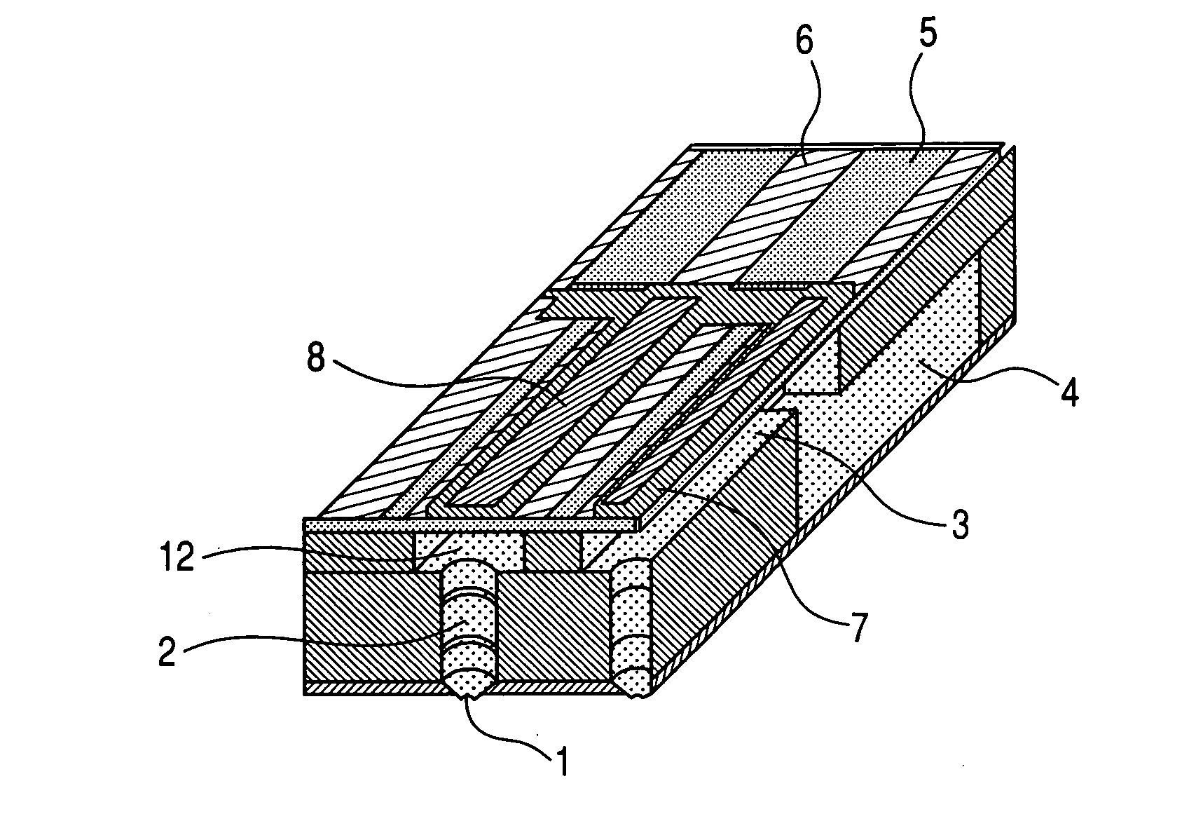
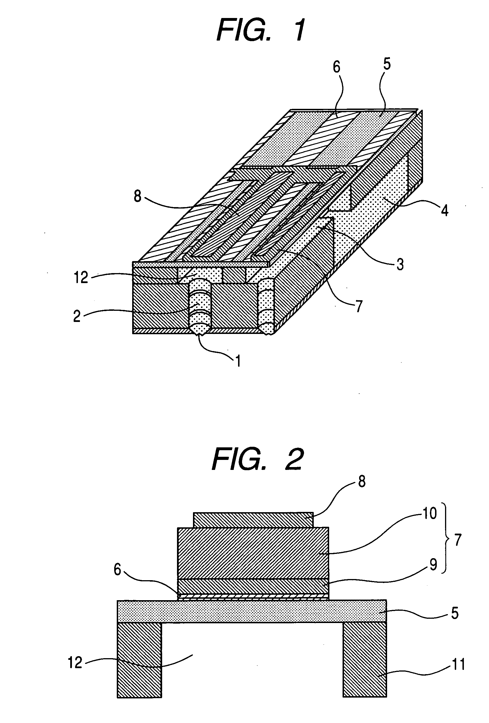
[0095] A Pt (100) orientation film was formed in 120-nm thickness on an MgO (100) substrate, and the first dielectric layer of the present invention was formed thereon in 10-nm thickness at substrate temperature of 590° C. by means of magnetron sputtering by using a target of which composition is Pb(Mg1 / 3Nb2 / 3)O3 and the Pb amount is excessive by 10 mole percent. The first layer was formed thereon by sequentially changing a Ti element against lead by 5 to 25 mole percent. The film thickness of the entire first layer is 50 nm.

[0096] The second dielectric layer of a PMN-PT layer ([Pb (Mg1 / 3Nb2 / 3)O3]0.67—[PbTiO3]0.33) was film-formed on the first layer at substrate temperature of 620° C., and the thin film of 100 nm with a good crystalline orientation was obtained. As for the target in this case, a green compact was used, which was created through heat treatment by mixing a powder of which PbTiO3 component is excessive by 100 percent with a PMN powder. To be more specific, ([Pb (Mg1 / 3...

sixth embodiments

Second to Sixth Embodiments

[0101] The ink jet head was created in the configuration described in Table 1 by changing the composition of each dielectric layer compared to the first embodiment. In any case, the thin film of a good (001) orientation could be obtained. However, the compositions in Table 1 are composition formulas. As a result of an ICP analysis, Pb is excessive in a range of 1.02 to 1.25, and the characteristics were especially good in that case. The ratio of compositions in the table are mole percentage values worth the lead of the slanted components for the lead. And the thickness of the first layer is the film thickness including the slanted structure portion.

TABLE 1COMPOSITION OF FIRST LAYERELEMENT OFCOMPOSITIONTHICKNESS OFEXAMPLEON THE SIDE OF ELECTRODESLANTED PORTIONRATIOFIRST LAYERε 12Pb(Zn1 / 3Nb2 / 3)O3La0.5˜2.0%0.06 μm660Ti0.5˜7.0%3Pb(Sc1 / 2Nb1 / 2)O3Ti2.0˜35%  0.1 μm7404Pb(Sc1 / 2Ta1 / 2)O3Ti2.0˜8.0%0.15 μm4805Pb(In1 / 2Nb1 / 2)O3Ti 5˜36%0.05 μm7806Pb(Ni1 / 3Nb2 / 3)O3Ca0.5˜1...

seventh embodiment

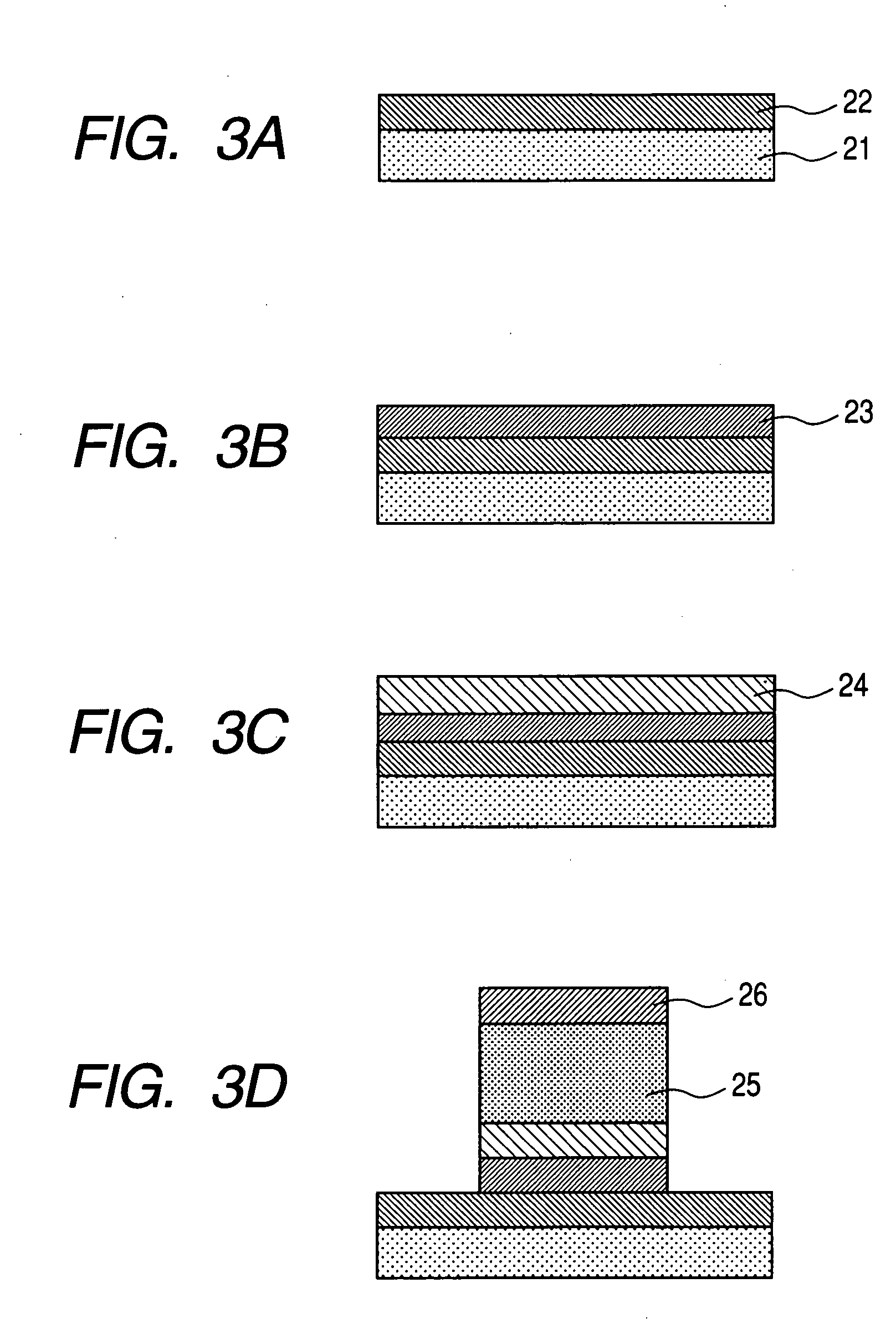
[0102] A YSZ (100) layer was film-formed in 0.1-μm thickness on the SOI layer by using the SOI substrate of which SOI (100) layer is 2 μm thick, SiO2 layer is 0.2 μm thick, handling layer Si (110) is 650 μm thick. An Ir (111) single-orientation film of 0.15 μm was formed thereon, the electrode-side composition of the first layer was Pb (Mg1 / 3Nb2 / 3)O3 and the slanted structure portion had the Ti element increased from 8 to 33 percent so that the entire film thickness was 0.2 μm. The second layer indicated by the composition formula of [Pb (Mg1 / 3Nb2 / 3)O3]0.67—[Pb0.7La0.3TiO3]0.33 was film-formed thereon in 2.5-μm thickness. The first layer was film-formed by using the target of which Pb component was excessive by 15 percent, and the second layer was film-formed by using the target of which composition was [Pb (Mg1 / 3Nb2 / 3)O3]0.67—[Pb0.7La0.3TiO3]0.6 and lead was excessive by 10 percent so as to obtain the piezoelectric layer of which second layer had the crystalline property of 89 perc...


PUM


Abstract

A dielectric element having a dielectric layer provided between an upper electrode layer and a lower electrode layer, wherein the dielectric layer has a first dielectric layer and a second dielectric layer mutually different in composition, and composition of at least one component of the first dielectric layer changes as to a thickness direction of the first dielectric layer in proximity to a boundary between the first dielectric layer and the second dielectric layer.

Description

BACKGROUND OF THE INVENTION [0001] 1. Field of the Invention [0002] The present invention relates to a dielectric element and a piezoelectric (electrostrictive) element capable of applications as MEMS in particular, such as a capacitor, a sensor, a transducer and an actuator as well as an ink jet head and an ink jet recording apparatus using the piezoelectric element. The present invention further relates to a manufacturing method thereof. [0003] 2. Related Background Art [0004] While a dielectric material of a high dielectric constant as a capacitor is in demand, thinning of ceramics materials such as BaTiO3 is underway for the sake of miniaturizing the capacitor. However, the dielectric constants of the ceramics materials such as BaTiO3 and Pb (Zr, Ti)O3 are only 1500 or so, and they often become electronic devices of defective characteristics when problems of improper sintering and a deficient structure of an interface are further added thereto by thinning them. [0005] As for a p...

Claims


Application Information

Patent Timeline
Patent Type & Authority Applications(United States)
IPC IPC(8): B41J2/01B41J2/045B41J2/055B41J2/135B41J2/14B41J2/145B41J2/16H01G4/12H01G4/33H01L41/18H01L41/187H01L41/22H01L41/316H02N2/00
CPCB41J2/14233B41J2202/03H10N30/8548H10N30/076H10N30/079A43C15/068
Inventor IFUKU, TOSHIHIROMATSUDA, TAKANORIAOKI, KATSUMITAKEDA, KENICHIWASA, KIYOTAKA
Owner CANON KK
Why Eureka
Try Eureka