
Apparatus for and method of noise suppression and dithering to improve resolution quality in a digital RF processor

Inactive Publication Date: 2005-08-25
TEXAS INSTR INC
View PDF7 Cites 112 Cited by
  • Summary
  • Abstract
  • Description
  • Claims
  • Application Information

AI Technical Summary

Benefits of technology

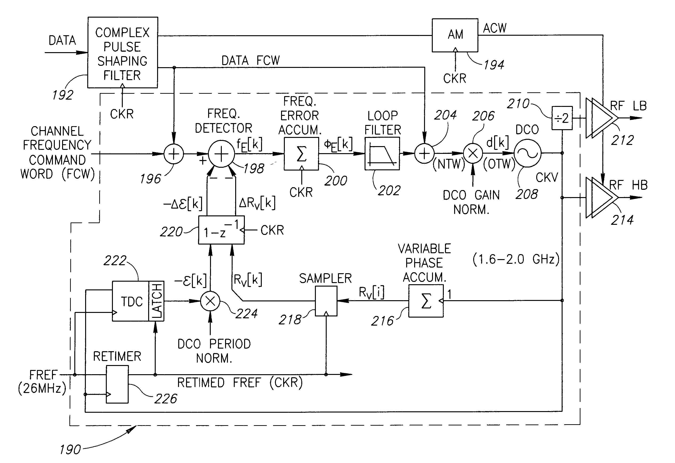
[0027] The present invention provides a solution to the problems of the prior art by providing an apparatus for and a method of noise suppression in a digital radio receiver and transmitter, or transceiver. This noise, including spurious tones, is particularly noticeable in a highly integrated CMOS based system on a chip (SoC) radio solution that incorporates a very large amount of digital content. The noise suppression scheme of the present invention is effective to eliminate the noise caused by the various on chip interference sources transmitted through power, ground and substrate paths. The noise suppression scheme permits an all digital PLL (ADPLL) to operate in such a way so as to avoid generating the spurs that would normally be generated from the injection pulling effect of interfering sources on the integrated circuit chip.
[0033] The present invention also comprises a method and apparatus of improving the resolution quality in a time to digital converter (TDC). The TDC is a component in the ADPLL that functions to measure the fractional time delay difference between the reference clock and the next rising edge of the RF oscillator clock. The quantization of timing estimation performed by the TDC affects the phase noise at the output of the ADPLL. The predominant contributor to TDC error is quantization noise. With proper design of the TDC, the noise in a deep-submicron CMOS process is low and it is expected to be sufficient for cellular applications. Operating the ADPLL at or near the integer-N channels, however, produces peculiar behavior due to the insufficient randomization of the TDC quantization noise.

Problems solved by technology

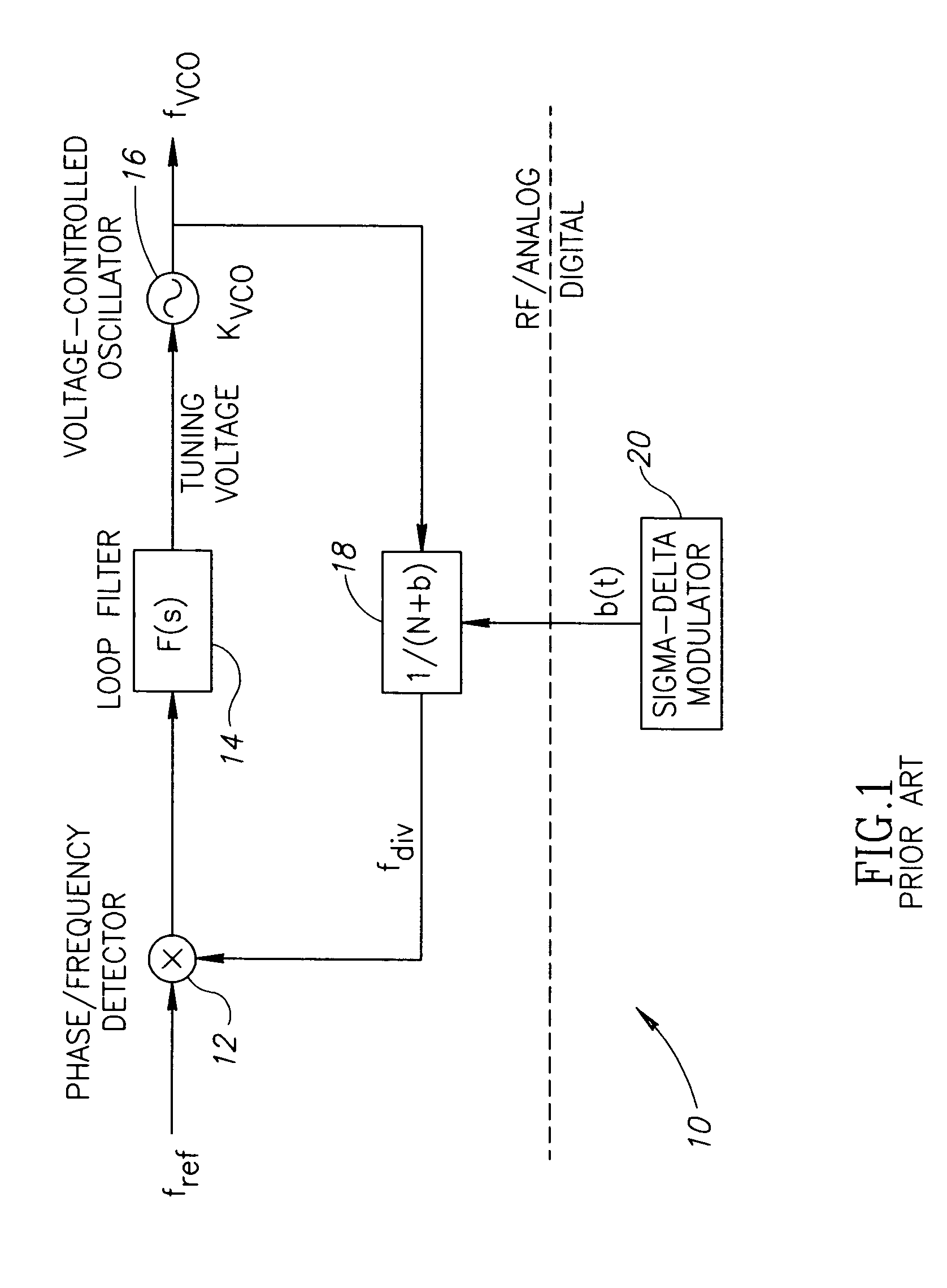
This noise, including spurious tones, is particularly noticeable in a highly integrated CMOS based system on a chip (SoC) radio solution that incorporates a very large amount of digital content.
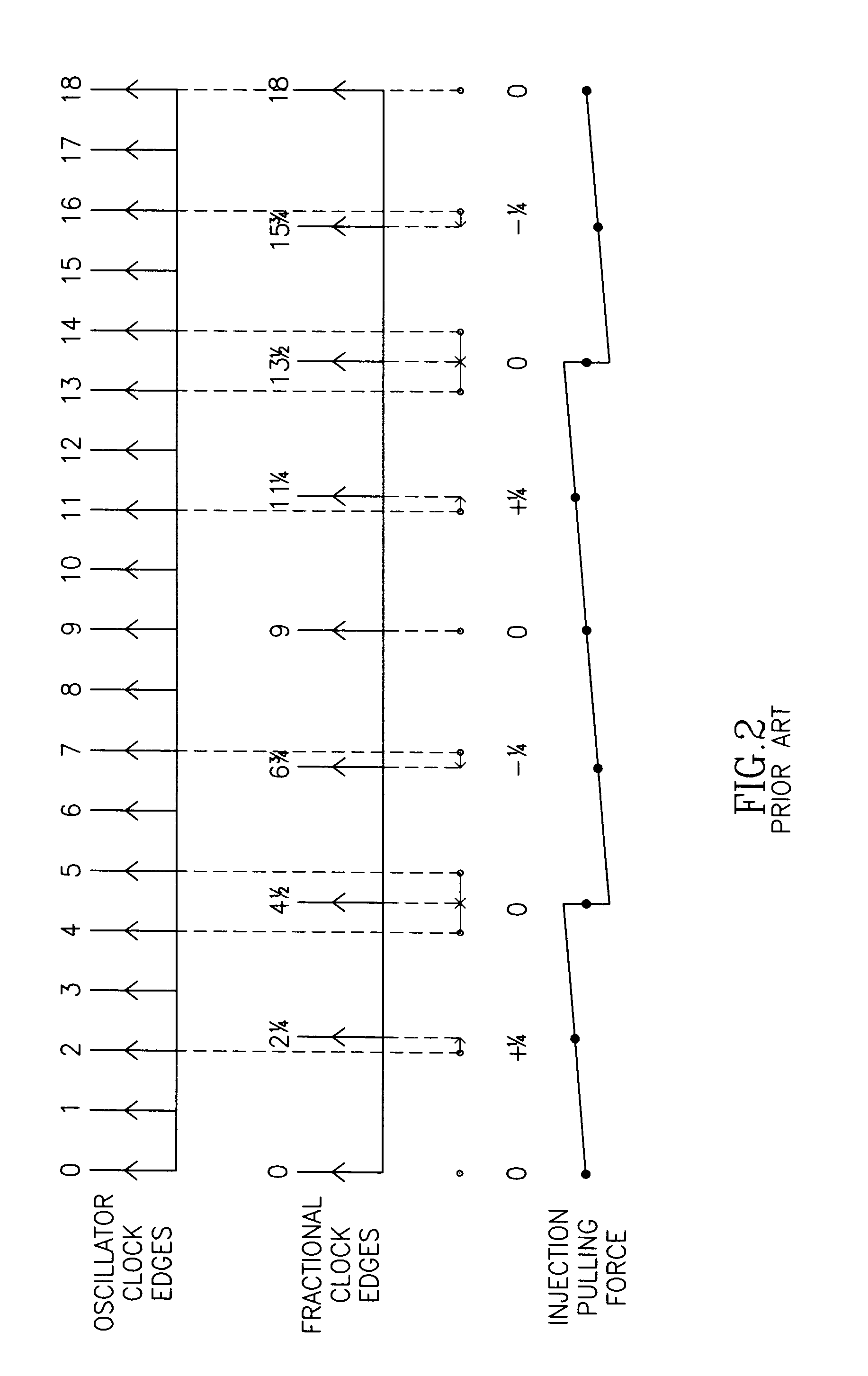
As described in the Background Section of this document, the mutual drift of the oscillator and clock edges is especially damaging to the system performance of the transmitter and the receiver because it subjects the RF oscillator to injection pulling forces and causes time varying noise coupling in sampled systems.
Such a solution would be very expensive and not likely to be as effective thus making it impractical to implement.

Method used


Image

  • Apparatus for and method of noise suppression and dithering to improve resolution quality in a digital RF processor
  • Apparatus for and method of noise suppression and dithering to improve resolution quality in a digital RF processor
  • Apparatus for and method of noise suppression and dithering to improve resolution quality in a digital RF processor

Examples


Embodiment Construction

Notation Used Throughout

[0056] The following notation is used throughout this document.

TermDefinitionA / DAnalog to DigitalACWAmplitude Control WordADPLLAll Digital Phase Locked LoopAMAmplitude ModulationASICApplication Specific Integrated CircuitCDMACode Division Multiple AccessCKRRetimed Reference ClockCKVVariable Oscillator ClockCMOSComplementary Metal Oxide SemiconductorDACDigital to Analog ConverterDCODigital Controlled OscillatorDCSDigital Communication ServicesDCXODigitally Controlled Crystal OscillatorDEMDynamic Element MatchingDRPDigital RF Processor or Digital Radio ProcessorDSPDigital Signal ProcessorFCWFrequency Command WordFPGAField Programmable Gate ArrayFREFFrequency ReferenceGSMGlobal System for Mobile CommunicationHBHigh BandHDLHardware Description LanguageICIntegrated CircuitIFIntermediate FrequencyLBLow BandLNALow Noise AmplifierLOLocal OscillatorPCSPersonal Communication ServicePLLPhase Locked LoopPVTProcess Voltage TemperatureRFRadio FrequencyRMSRoot Mean Squar...


PUM


Abstract

A novel apparatus for and a method of noise and spurious tones suppression in a digital RF processor (DRP). The invention is well suited for use in highly integrated system on a chip (SoC) radio solutions that incorporate a very large amount of digital logic circuitry. The noise suppression scheme eliminates the noise caused by various on chip interference sources transmitted through electromagnetic, power, ground and substrate paths. The noise suppression scheme permits an all digital PLL (ADPLL) to operate in such a way to avoid generating the spurs that would normally be generated from the injection pulling effect of interfering sources on the chip. The frequency reference clock is retimed to be synchronous to the RF oscillator clock and used to drive the entire digital logic circuitry of the DRP. This ensures that the different clock edges throughout the system will not exhibit mutual drift. A method of improving the resolution quality of a time to digital converter within the ADPLL is also taught. The method dithers the reference clock by passing it through a delay circuit that is controlled by a sigma-delta modulator. The dithered reference clock reduces the affect on the phase noise at the output of the ADPLL due to ill-behaved quantization of the TDC timing estimation.

Description

REFERENCE TO RELATED APPLICATIONS [0001] This application claims priority to U.S. Provisional Application Ser. No. 60 / 546,249, filed Feb. 19, 2004, entitled “Clock Retiming and Synchronization Method for Noise Suppression in the Digital Radio Processor”, incorporated herein by reference in its entirety.FIELD OF THE INVENTION [0002] The present invention relates to the field of data communications and more particularly relates to an apparatus for and method of suppressing noise in a digital RF processor (DRP)™ and an apparatus for and method of dithering to improve the resolution quality of a time to digital converter in a DRP. BACKGROUND OF THE INVENTION [0003] It is well known that oscillatory systems are susceptible to injection pulling and injection locking. As an example, it has been observed that humans left in isolated bunkers reveal a free running sleep-wake period of about 25 hours. A natural day on Earth is 24 hours, however, and humans exposed to this 24-hour cycle are inj...

Claims


Application Information

Patent Timeline
IPC IPC(8): H03C3/00H03L7/16H04B1/04H04B1/06H04B1/68
CPCH03L2207/50H03L7/16
Inventor STASZEWSKI, ROBERT B.LEIPOLD, DIRKMUHAMMAD, KHURRAMREZEQ, SAMEH S.
Owner TEXAS INSTR INC
Learn More