
Solid-state imaging apparatus having multiple anti-reflective layers and method for fabricating the multiple anti-reflective layers

Inactive Publication Date: 2005-08-25
SAMSUNG ELECTRONICS CO LTD
View PDF4 Cites 56 Cited by
  • Summary
  • Abstract
  • Description
  • Claims
  • Application Information

AI Technical Summary

Benefits of technology

[0013] The present invention provides a solid-state imaging apparatus comprising multiple anti-reflective layers which can improve a smear characteristic while suppressing a dark defect.
[0014] The present invention also provides a method for fabricating the multiple anti-reflective layers of a solid-state imaging apparatus, which can improve a smear characteristic while suppressing a dark defect.

Problems solved by technology

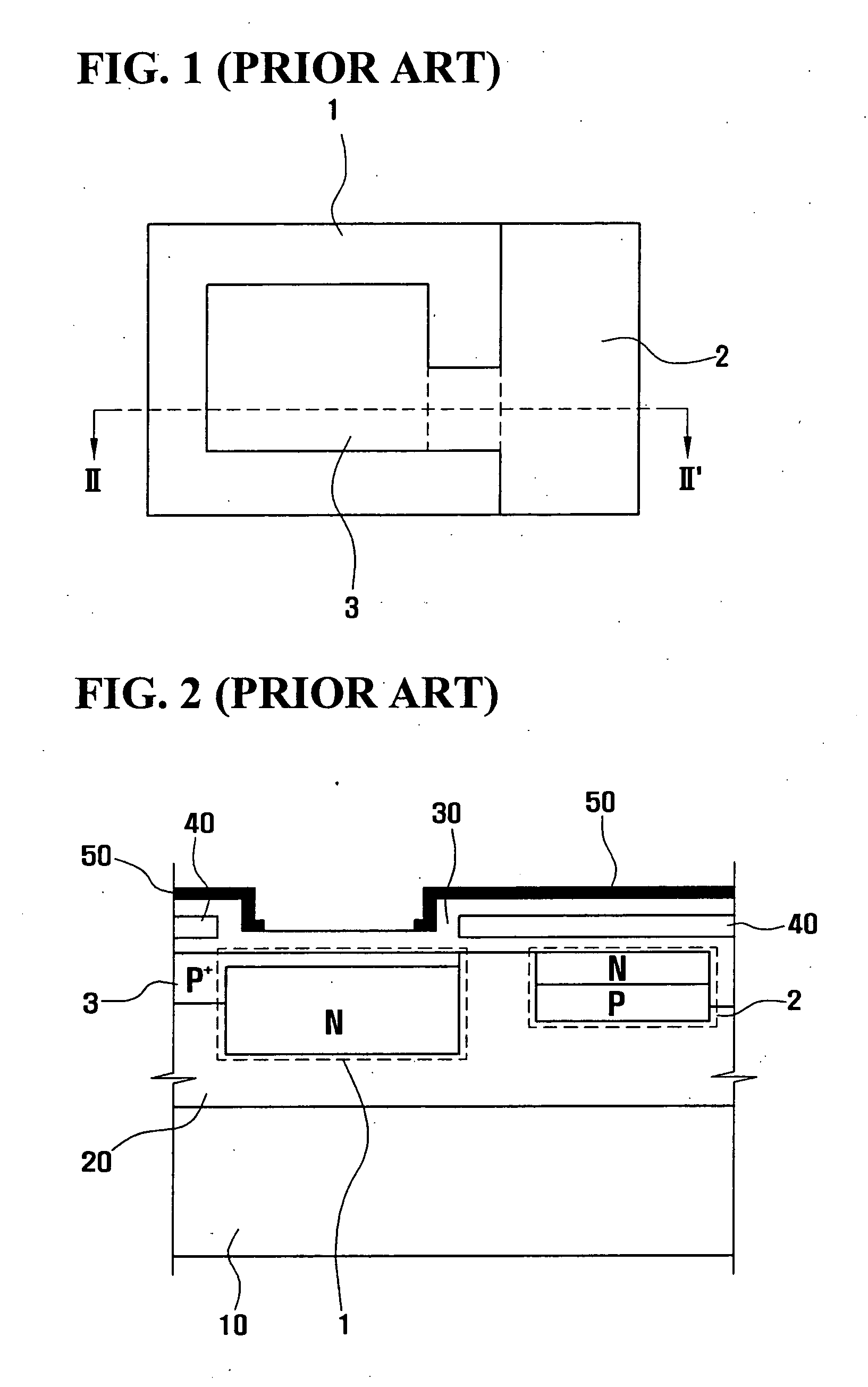
If the anti-reflective layer is first formed on the entire surface of the semiconductor substrate 10 having the light receiving element 1 and the charge transfer element 2 and the shading layer 50 is then formed thereon, a thickness of a layer underlying the shading layer 50 undesirably increases, which may generate an erroneous image charge signal due to diffused reflection of light incident to a portion surrounding the light receiving element 1, and cause noise, thereby resulting in a deterioration in smear components.
However, when the anti-reflective layer is selectively removed by dry etching, damage may occur to the semiconductor substrate 10 due to plasma generated during dry etching.
Accordingly, a dark defect phenomenon may appear due to such plasma damage.
Thus, it is quite difficult to uniformly control smearing characteristics occurring in multiple light receiving elements.

Method used


Image

  • Solid-state imaging apparatus having multiple anti-reflective layers and method for fabricating the multiple anti-reflective layers
  • Solid-state imaging apparatus having multiple anti-reflective layers and method for fabricating the multiple anti-reflective layers
  • Solid-state imaging apparatus having multiple anti-reflective layers and method for fabricating the multiple anti-reflective layers

Examples


Embodiment Construction

[0033] In the following detailed description, whenever a layer or structure is referred to as “on” another layer or structure, the first layer or structure may be directly on the second layer or structure, or other intervening layers or structures may be present.

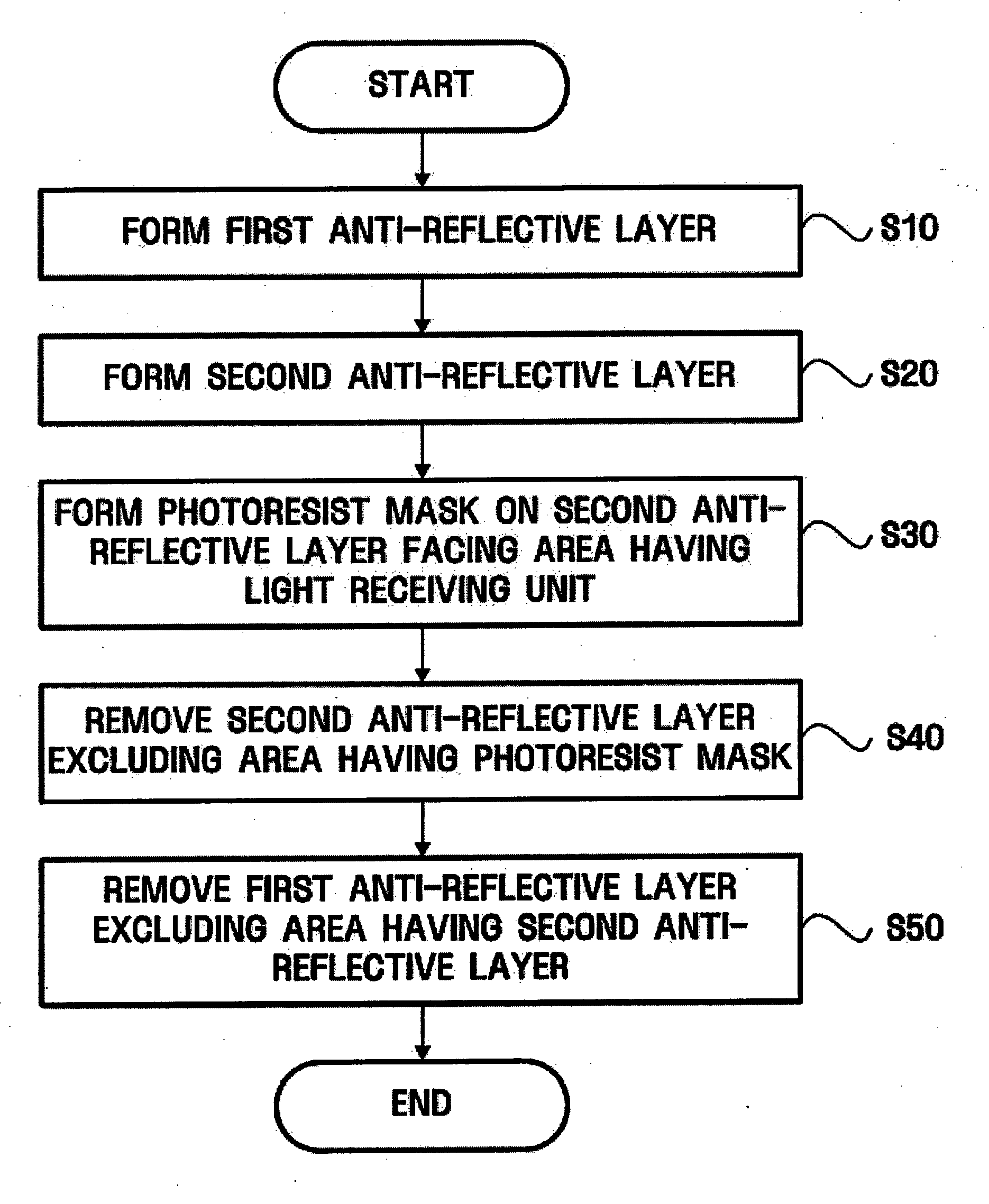
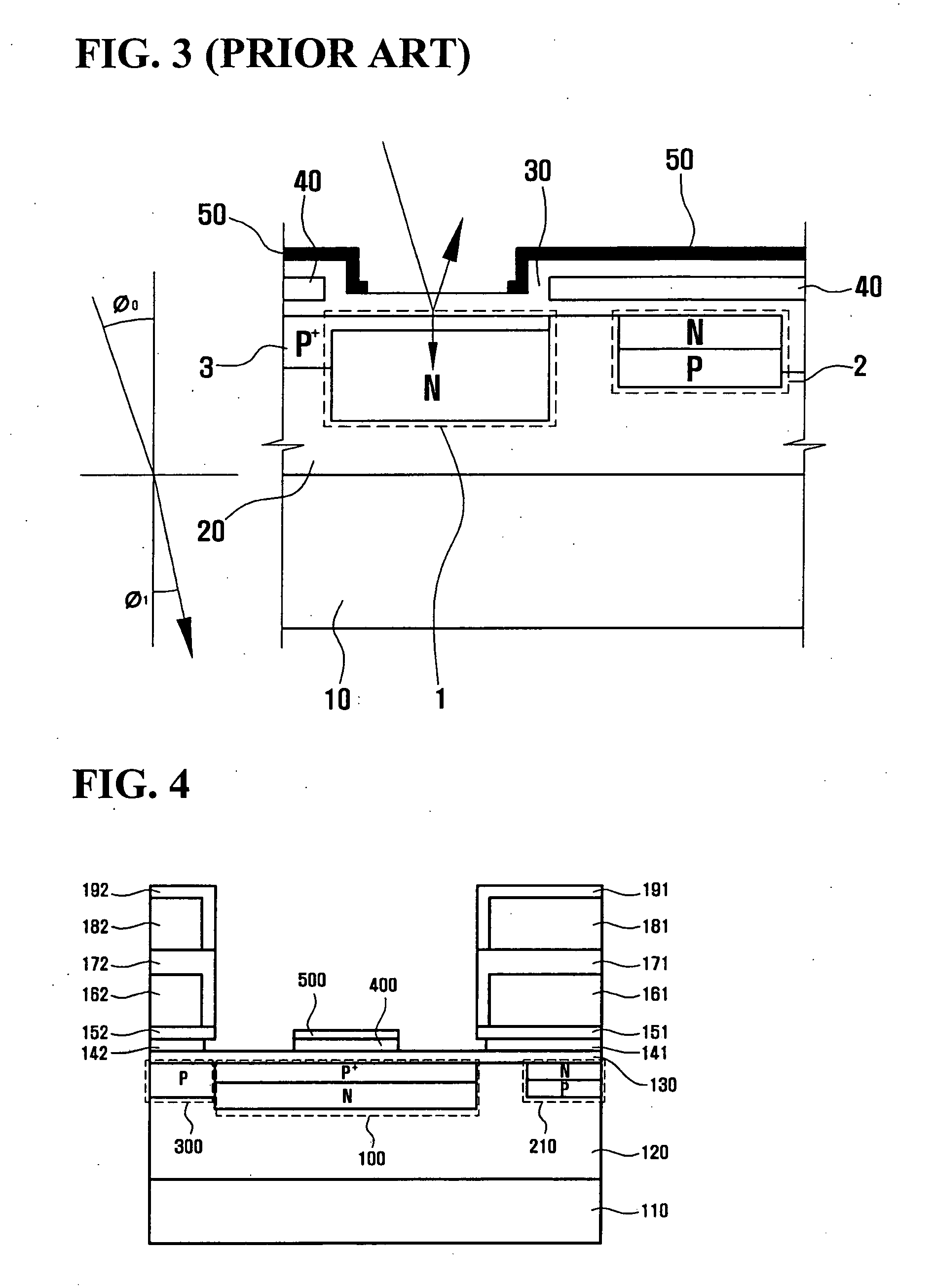
[0034] Referring to FIGS. 4, 5, and 6A through 6F, a solid-state imaging apparatus comprising multiple anti-reflective layers according to the present invention, which has improved smear correction capability while suppressing dark defects, will now be described.

[0035]FIG. 4 is a cross-sectional view of a solid-state imaging apparatus according to an embodiment of the present invention, FIG. 5 is a flowchart illustrating a method for fabricating multiple anti-reflective layers of the solid-state imaging apparatus according to the present invention, and FIG. 6A through FIG. 6F are cross-sectional views showing the method for fabricating the multiple anti-reflective layers of solid-state imaging apparatus according to the pr...


PUM


Abstract

A solid-state imaging apparatus comprising multiple anti-reflective layers which can improve a smear characteristic while suppressing a dark defect and a method for fabricating the multiple anti-reflective layers are provided. The solid-state imaging apparatus includes a light receiving unit, a charge transfer unit, and multiple anti-reflective layers. The method includes forming a first anti-reflective layer, forming a second anti-reflective layer, forming a photoresist mask, removing the second anti-reflective layer, and removing the first anti-reflective layer.

Description

[0001] This application claims priority from Korean Patent Application No. 10-2004-0012763 filed on Feb. 25, 2004 in the Korean Intellectual Property Office, the contents of which are incorporated herein by reference. BACKGROUND OF THE INVENTION [0002] 1. Field of the Invention [0003] The present invention relates to a solid-state imaging apparatus having a multiple anti-reflective layers and a method for fabricating the multiple anti-reflective layers, more particularly, to a solid-state imaging apparatus having multiple anti-reflective layers which improve a smear characteristic while suppressing a dark defect, and a method for fabricating the multiple anti-reflective layers. [0004] 2. Description of the Related Art [0005] In recent years, attention has focused on a solid-state imaging apparatus for use in camcorders, mobile phones, digital cameras, and so on, as an electronic eye. In general, a solid-state imaging apparatus includes a light receiving element for converting a sign...

Claims


Application Information

Patent Timeline
IPC IPC(8): G03C5/00H01L21/76H01L21/8238H01L23/544H01L27/148H01L27/146H01L31/10
CPCH01L27/14601H01L27/14685H01L27/1462B25B21/00B25F5/001
Inventor KIM, HONG-KI
Owner SAMSUNG ELECTRONICS CO LTD
Learn More