Semiconductor package for lowering electromagnetic interference and method for fabricating the same

a technology of electromagnetic interference and semiconductor packages, which is applied in the direction of semiconductor devices, semiconductor/solid-state device details, electrical apparatus, etc., can solve the problems of reducing the electrical performance severe electromagnetic wave problem, and large amount of heat, so as to improve the electrical quality and heat dissipation efficiency of the semiconductor package, and reduce the fabrication cost and package weight. , the effect of lowering electromagnetic interferen

Inactive Publication Date: 2005-08-25
STACK DEVICES CORP
View PDF0 Cites 29 Cited by
  • Summary
  • Abstract
  • Description
  • Claims
  • Application Information

AI Technical Summary

Benefits of technology

[0008] A primary objective of the present invention is to provide a semiconductor package for lowering electromagnetic interference (EMI) and a method for fabricating the same, by which electromagnetic waves are converted to heat to reduce the EMI.
[0009] Another objective of the present invention is to provide a semiconductor package for lowering EMI and a method for fabricating the same, by which the semiconductor package has excellent heat dissipation effect.
[0010] Still another objective of the present invention is to provide a semiconductor package for lowering EMI and a method for fabricating the same, by which the semiconductor package is cost-effective and simple to be fabricated.
[0011] A further objective of the present invention is to provide a semiconductor package for lowering EMI and a method for fabricating the same, by which the semiconductor package has a reduced weight.
[0012] A further objective of the present invention is to provide a semiconductor package for lowering EMI and a method for fabricating the same, by which the semiconductor package has ideal electrical quality.
[0016] The semiconductor package for lowering electromagnetic interference and the method for fabricating the same proposed in the present invention employ an electromagnetic absorbing layer having a plurality of porous metal particles for absorbing electromagnetic waves from the chip and converting the absorbed electromagnetic waves into heat that can be dissipated. The present invention not only solves the problem of electromagnetic interference without having to use the conventional metal mask, but also significantly improves the electrical quality and heat dissipation efficiency of the semiconductor package as well as provides advantages such as reduction of the fabrication cost and the package weight, such that the prior-art drawbacks are eliminated.

Problems solved by technology

However, a severe problem of electromagnetic waves is usually caused during the operation of the foregoing semiconductor chip.
This situation may further degrade the electrical performance and heat dissipation effect of the semiconductor package.
These electromagnetic waves 75 may not only influence the quality of electrical transmission between the chip 61 and the bonding wires 64 but also generate a large amount of heat in the encapsulation body 66 due to energy attenuation of the electromagnetic waves 75, thereby leading to a heavy burden on heat dissipation of the semiconductor package.
Additionally, the metal mask 70 usually has a relatively larger weight and higher material cost, and its mounting method cannot be performed through automatic mass production.
Thus, the use of the metal mask 70 does not comply with the development trends such as light weight, low cost and high mass production of semiconductor packages, which is considered a trouble for packaging high-frequency chips.

Method used


Image

  • Semiconductor package for lowering electromagnetic interference and method for fabricating the same
  • Semiconductor package for lowering electromagnetic interference and method for fabricating the same
  • Semiconductor package for lowering electromagnetic interference and method for fabricating the same

Examples


Embodiment Construction

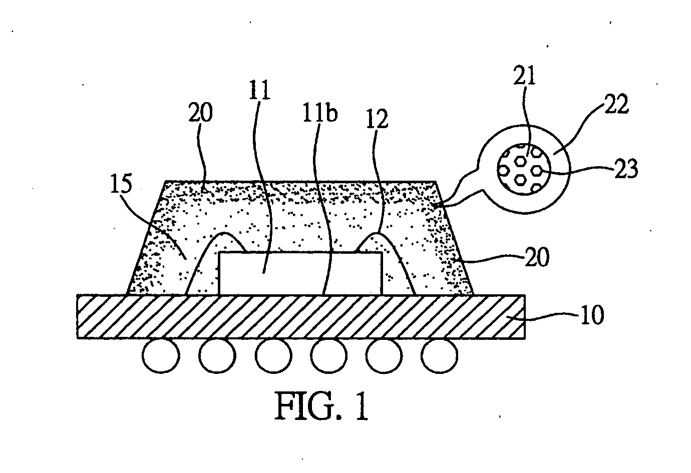
[0027] The preferred embodiments of a semiconductor package for lowering electromagnetic interference (EMI) and a method for fabricating the same proposed in the present invention are described in the following with reference to FIGS. 1 to 6.

[0028] The semiconductor packages according to a first preferred embodiment of the present invention is shown in FIG. 1, using a substrate 10 as a chip carrier. A high-frequency chip 11 is mounted with its inactive surface 11b on the substrate 10 and electrically connected to a conductive trace layer (not shown) of the substrate 10a via a plurality of bonding wires 12. An encapsulation body 15 made of a resin material such as an epoxy resin is formed on the substrate 10 to encapsulate the chip 11 and the bonding wires 12. The encapsulation body 15 comprises an electromagnetic absorbing layer 20 for absorbing electromagnetic waves generated by the chip 11 and converting the absorbed electromagnetic waves into heat. In this embodiment, the electr...


PUM


Abstract

A semiconductor package for lowering electromagnetic interference and a method for fabricating the same are proposed. The semiconductor package includes a chip carrier, at least one chip attached and electrically connected to the chip carrier, and an encapsulation body formed on the chip carrier for encapsulating the chip. The encapsulation body includes an electromagnetic absorbing layer made of an organic material filled with a plurality of porous metal particles. The electromagnetic absorbing layer absorbs electromagnetic waves generated by the chip and converts the electromagnetic waves to heat so as to improve the heat dissipation efficiency and reduce electromagnetic interference for the semiconductor package.

Description

PRIOR APPLICATION DATA [0001] The present application claims benefit from prior Taiwan, R.O.C. application serial number 093104545 filed on Feb. 24, 2004. FIELD OF THE INVENTION [0002] The present invention relates to semiconductor packages for lowering electromagnetic interference and methods for fabricating the same, and more specifically, to a semiconductor package in which electromagnetic waves are converted to heat and dissipated to lower the electromagnetic interference, and a fabrication method of the semiconductor package. BACKGROUND OF THE INVENTION [0003] With the rapid development of electronic and digital industry, functional requirements of electronic products become more demanded. Therefore, researchers directed to semiconductor packages have focused on ways to improve the techniques of semiconductor fabrication and integrated circuit design to fabricate high-frequency chips with more functionality. For a semiconductor package using a high-frequency chip, conventionall...

Claims


Application Information

Patent Timeline
IPC IPC(8): H01L23/26H01L23/28H01L23/29H01L23/31H01L23/552
CPCH01L23/295H01L23/3121H01L2224/73204H01L2224/32225H01L2224/16227H01L2224/16225H01L24/48H01L2924/3025H01L2924/15311H01L2224/48247H01L23/552H01L2224/48227H01L2924/00H01L2924/14H01L2924/181H01L2924/00014H01L2924/00012H01L2224/45099H01L2224/45015H01L2924/207
Inventor BAI, JIN-CHUNGHUANG, CHI-PANG
Owner STACK DEVICES CORP
Why Eureka
Try Eureka