
Flexible printed circuit board

a printed circuit board and flexible technology, applied in the field of flexible printed circuit boards, can solve the problems of reducing the uneven breakage of conductive particles, etc., and achieve good reliability of anisotropic conductive films

Inactive Publication Date: 2005-08-25
ARIMA DISPLAY
View PDF6 Cites 72 Cited by
  • Summary
  • Abstract
  • Description
  • Claims
  • Application Information

AI Technical Summary

Benefits of technology

"The present invention provides a flexible printed circuit board with an anisotropic conductive film for use in handheld electrical devices. The conductive film has even and low impedance, and is reliable for use in such devices. The circuit board has a broader pitch of the conductive film layer, which helps to achieve better reliability. The conductive film includes conductive particles and sticky polymers, and the substrate layer is a plastic layer. The circuit board can be connected to a liquid crystal display or other electronic components using the conductive film layer."

Problems solved by technology

However, the conductive particles are often broken unevenly.
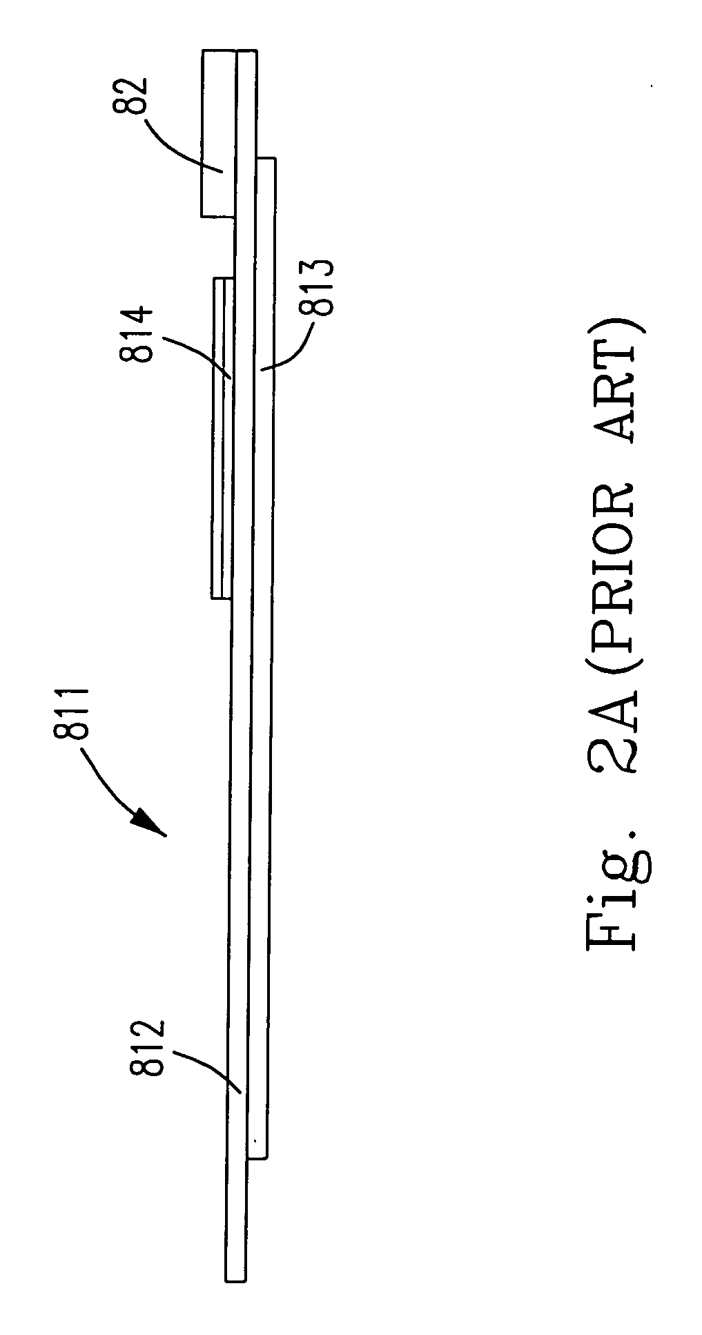
Though the conductive particles of uneven breakage can still conduct electricity, they could reduce the reliability of the anisotropic conductive film 8121.
As a result, the anisotropic conductive film 8121 is not smooth, which causes the uneven breakage of the conductive particles.

Method used


Image

  • Flexible printed circuit board
  • Flexible printed circuit board
  • Flexible printed circuit board

Examples


first embodiment

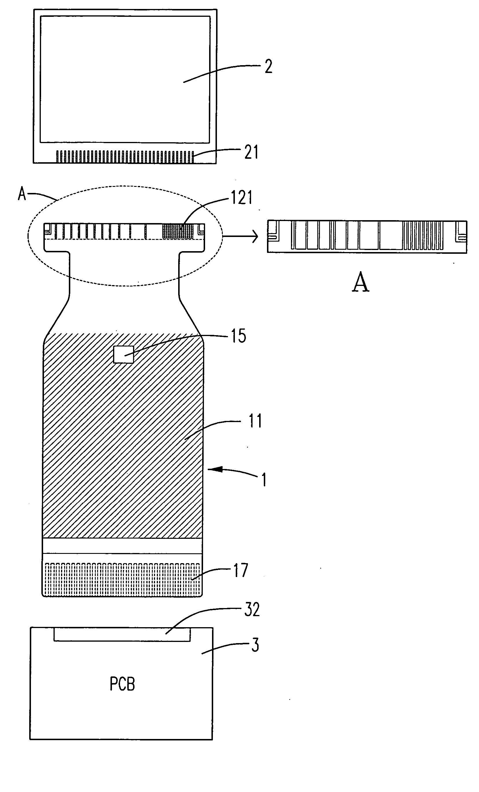
[0044] The present invention will now be described more specifically with reference to the following embodiments. In the present invention, the flexible printed circuit boards 1, 1′ with the broadened anisotropic conductive film respectively have the main portions 11, 11′. Please refer to FIGS. 3A and 4A, which are side views showing the main portions of the flexible printed circuit boards according to the preferred embodiments of the present invention. The main portions 11, 11′ are respectively made up of the first circuit layers (circuit layer) 13, 13′, the second circuit layers (circuit layer) 14, 14′, and the plastic layers (substrate layer) 12,12′. Preferably, the plastic layers 12, 12′ can be polyimide having good flexibility and mechanical property, i.e. all-polyimide flexible printed circuit board. In addition, a polypropylene / epoxy resin layer can be spread on the polyimide layer. Preferably, the first and the second circuit layers 13, 13′, 14, 14′ are printed copper layers...

second embodiment

[0047] In the present invention, the flexible printed circuit boards 1, 1′ are all-polyimide flexible laminae. For example, it has two layers, three layers, four layers, and six layers.

[0048] Please refer to FIG. 5 which is a side view of FIG. 3B showing the liquid crystal display of the handheld electronic devices. In the left side, the drawing is the liquid crystal display 2, whose up-right portion is the indium-tin oxide layer 21, 21′. The indium-tin oxide layer 21, 21′ is electrically connected to the anisotropic conductive film 121 located at down-left portion of the flexible printed circuit board 1 by the bonding process. Moreover, the substrate layer 12, the circuit layer 13, and integrated circuit 15 are also shown in the drawing.

[0049] In the anisotropic conductive adhesive or anisotropic conductive films 121, 121′ of the present invention, usually the conductive particles are dispersed and mixed in the polymers in a random fashion. The sticky polymers are subsequently tra...


PUM


Abstract

A flexible printed circuit with a broadened anisotropic conductive film is provided. The flexible printed circuit includes a substrate layer and a circuit layer, characterized in that a pitch of the anisotropic conductive film is broadened to be ranged from 0.5 mm to 3.0 mm. It has even and low impedance, even breakage of conductive particles, even pressure, and thus has good reliability of the anisotropic conductive film for use in handheld electronic devices.

Description

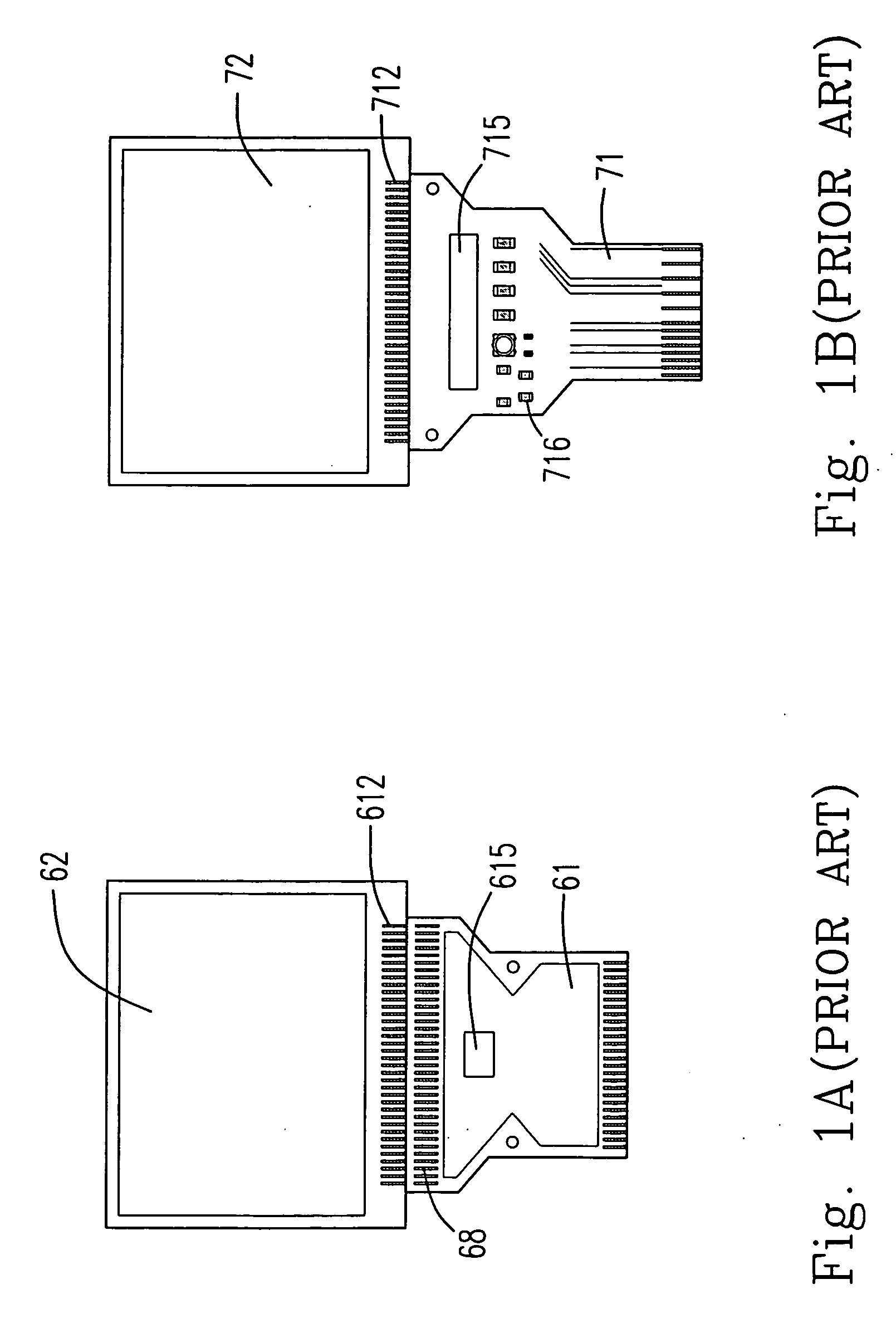
FIELD OF THE INVENTION [0001] The present invention relates to a flexible printed circuit board, particularly to a flexible printed circuit board with an anisotropic conductive film, which has even and low impedance, even breakage of conductive particles, even pressure, and thus has good reliability of the anisotropic conductive film for use in handheld electrical devices. BACKGROUND OF THE INVENTION [0002] Please refer to FIG. 1A and FIG. 1B. They are schematic views showing the liquid crystal display devices provided in the industry with the prevalence of handheld electrical devices, such as cellular phone, PDA, smart phone, stock manager, etc. In the drawings, the flexible printed circuit boards 61, 71 can be built with a copper circuit print and can be fixed with integrated circuits 615, 715 respectively. The surface mounting devices (SMD) 716 (such as surface mounting capacitor, surface mounting resistor, LED and etc.) can be mounted on the flexible printed circuit board 71 as ...

Claims


Application Information

Patent Timeline
Patent Type & Authority Applications(United States)
IPC IPC(8): H05K3/32H05K3/36
CPCH05K3/323H05K2201/09781H05K3/361
Inventor SU, PI-CHUAN
Owner ARIMA DISPLAY
Learn More