
Method and apparatus for reducing leakage current in a read only memory device using transistor bias

a technology of read only memory and leakage current, applied in the field of leakage current reduction of electronic memory devices, can solve the problems of high leakage current, transistor sub-threshold leakage current, and significant leakage current of transistor sub-threshold, and achieve the effect of reducing leakage current and reducing leakage curren

Active Publication Date: 2005-07-28
AVAGO TECH INT SALES PTE LTD
View PDF7 Cites 2 Cited by
  • Summary
  • Abstract
  • Description
  • Claims
  • Application Information

AI Technical Summary

Benefits of technology

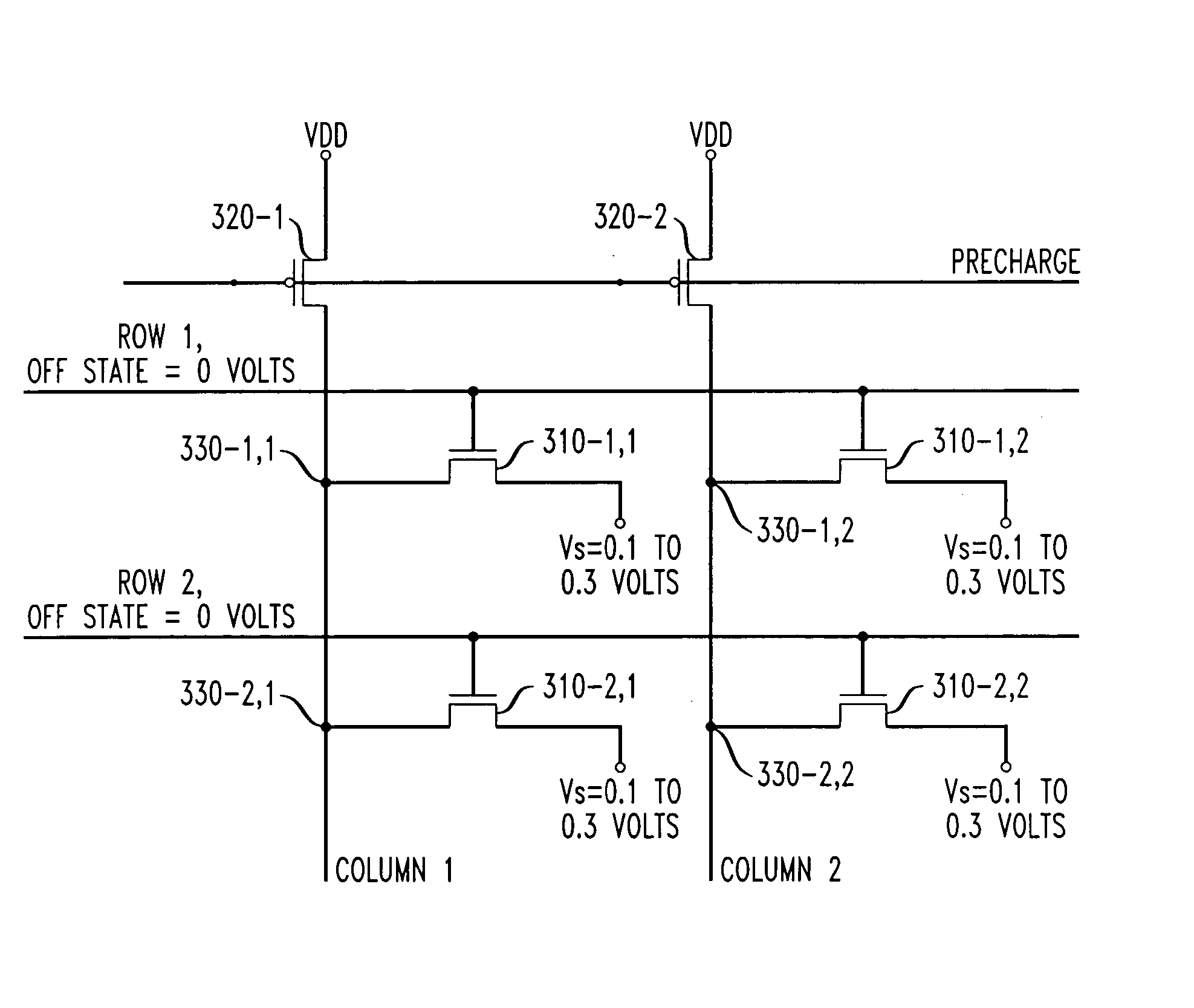
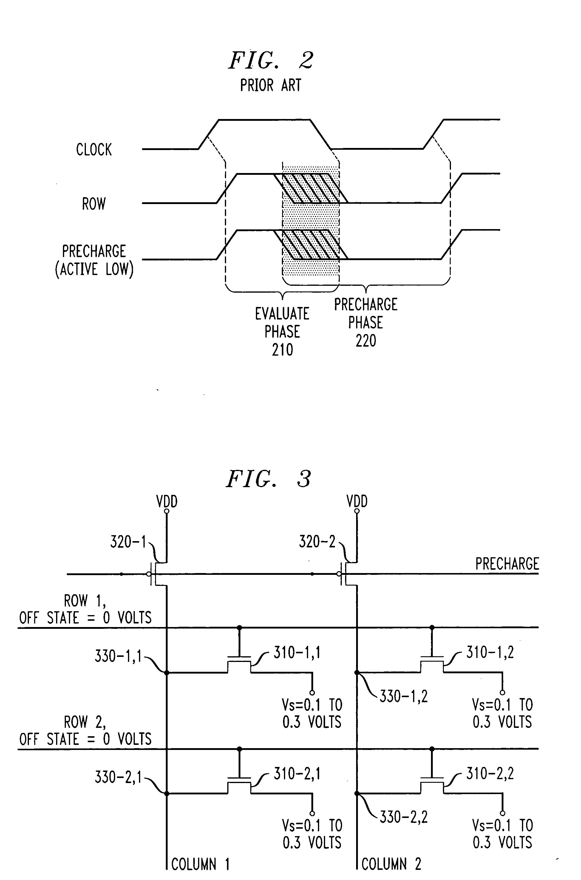
[0006] Generally, a method and apparatus are provided for reducing leakage current in a read only memory device. The present invention reduces leakage current in a read only memory array by applying a biased gate voltage (relative to a source voltage) to the gate of at least one of transistor in the array. The biased gate voltage is applied at least during a precharge phase of a read cycle. When the array transistors are n-channel transistors, the biased voltage is a negative bias voltage (relative to the source voltage). When the array transistors are p-channel transistors, the biased voltage is a positive bias voltage (relative to the source voltage).
[0007] In an exemplary implementation of the invention employing n-channel transistors, the reduced off-state gate voltage (below the source voltage) reduces n-channel transistor subthreshold leakage current. Applying a negative backgate bias to the transistor's p-well contact can also reduce n-channel transistor subthreshold leakage current. Thus, for an n-channel array, a negative gate voltage and backgate bias (optional) are applied to cell transistors in the off state by raising the source of programmed cell transistors from typically 0 volts (ground) to a small positive potential (typically 0.1 volts). Similarly, the subthreshold leakage current of p-channel transistors is reduced by applying a more positive gate-to-source bias and a positive n-well-to-source bias.

Problems solved by technology

As the size of ROM memory devices decrease, with improvements in integrated circuit fabrication technologies, the more narrow trace widths and shorter channel lengths of the ROM memory cell transistors can cause high leakage currents, referred to as transistor sub-threshold leakage current.
With more advanced CMOS technologies having trace widths of 0.16 μm or less, however, the transistor sub-threshold leakage current becomes a significant problem.
Such techniques, however, cause an undesirable increase in the physical size of the memory device, reduce the maximum frequency of operation and increase the active and standby currents.

Method used


Image

  • Method and apparatus for reducing leakage current in a read only memory device using transistor bias
  • Method and apparatus for reducing leakage current in a read only memory device using transistor bias
  • Method and apparatus for reducing leakage current in a read only memory device using transistor bias

Examples


Embodiment Construction

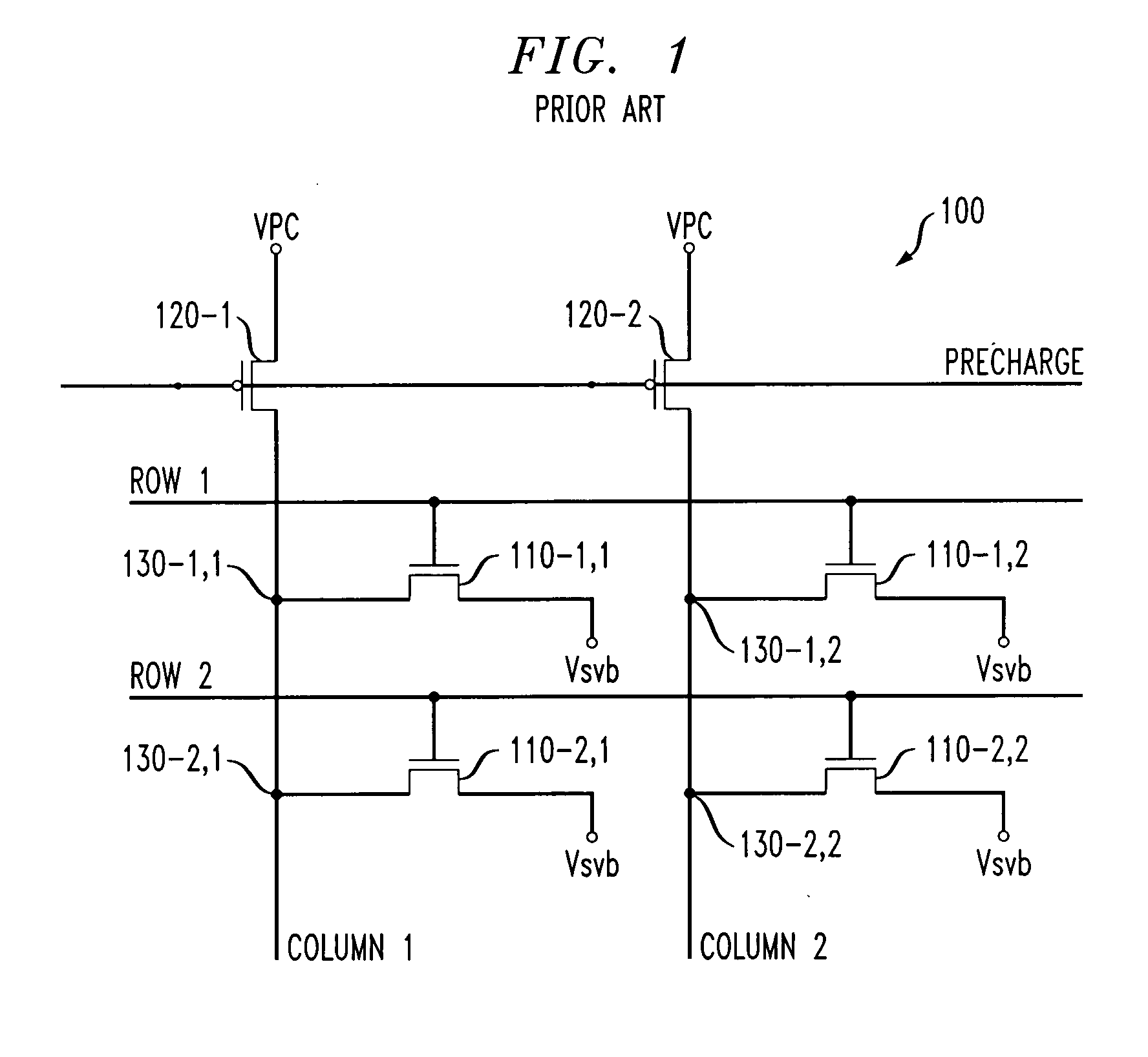
[0014]FIG. 1 illustrates a conventional two by two ROM array 100 of memory cells 110-1,1 through 110-i, j. The memory cells 110-1,1 through 110-i, j are generally comprised of transistors generally arranged in a grid pattern having a plurality (or series) of rows and columns. As shown in FIG. 1, the exemplary ROM array 100 includes a plurality, i, of rows (i=2), and a plurality, j, of columns (j=2). Each memory cell 110 has an associated programmable contact window 130-i,j that may optionally be programmed during the fabrication process.

[0015] Each column is supplied with power (VPC) at a first predetermined voltage level, often referred to as the “pre-charged voltage level,” and each row is supplied with power at a second predetermined voltage level. Values for these first and second predetermined voltage levels typically depend upon the selected ROM implementation. For example, when the transistors 110 of the array 100 are n-channel, the column is typically pre-charged to a first...


PUM


Abstract

A method and apparatus are provided for reducing leakage current in a read only memory device. Leakage current is reduced by applying a biased gate voltage (relative to a source voltage) to the gate of at least one of transistor in the array. The biased gate voltage is applied at least during a precharge phase of a read cycle. When the array transistors are n-channel transistors, the biased voltage is a negative bias voltage (relative to the source voltage). When the array transistors are p-channel transistors, the biased voltage is a positive bias voltage (relative to the source voltage). Applying a negative backgate bias to the transistor's p-well contact can also reduce n-channel transistor subthreshold leakage current. Thus, for an n-channel array, a negative gate voltage and backgate bias (optional) are applied to cell transistors in the off state. Similarly, the subthreshold leakage current of p-channel transistors is reduced by applying a more positive gate-to-source bias and a positive n-well-to-source bias.

Description

CROSS-REFERENCE TO RELATED APPLICATION [0001] The present application is related to U.S. patent application Ser. No. ______, entitled “Method and Apparatus for Reducing Leakage Current in a Read Only Memory Device Using Shortened Precharge Phase,” (Attorney Docket No. Dudeck 1-4-32-5), and U.S. patent application Ser. No. ______, entitled “Method and Apparatus for Reducing Leakage Current in a Read Only Memory Device Using Pre-Charged Sub-Arrays,” (Attorney Docket No. Dudeck 2-5-33-6), each filed contemporaneously herewith and incorporated by reference herein.FIELD OF THE INVENTION [0002] The present invention relates generally to electronic memory devices, and more particularly to the reduction of leakage current in electronic memory devices comprised of arrays of transistors. BACKGROUND OF THE INVENTION [0003] Data storage devices, such as read only memories (“ROMs”), typically store data in arrays of memory cells. Generally, a memory cell consists of a single transistor for each ...

Claims


Application Information

Patent Timeline
IPC IPC(8): G11C7/12G11C17/00G11C17/12
CPCG11C17/12G11C7/12
Inventor DUDECK, DENNIS E.EVANS, DONALD ALBERTKOHLER, ROSS ALANMCPARTLAND, RICHARD JOSEPHPHAM, HAI QUANG
Owner AVAGO TECH INT SALES PTE LTD
Learn More