
Populated printed wiring board and method of manufacture

a printed circuit board and printed circuit board technology, applied in the manufacture of final products, manufacturing tools, electrical apparatus construction details, etc., can solve the problems of conflicting demands on the soldering process, large cost of miniaturizing the microchip, and large external connection requirements of high-integrated microchips

Active Publication Date: 2005-07-21
GOOGLE TECH HLDG LLC
View PDF16 Cites 23 Cited by
  • Summary
  • Abstract
  • Description
  • Claims
  • Application Information

AI Technical Summary

Problems solved by technology

Highly integrated microchips often require a large number of external connections.
Thus, even though the microchip itself is highly miniaturized, a large package is necessitated, thereby negating, in certain respects the great expense incurred in miniaturizing the microchip.
However, the inclusion of disparate types of devices places conflicting demands on the soldering process by which components are secured to the PWB.
RFI / EMI shields present their own challenges to the solder process.
Addressing the imperfections in the flatness of the shield calls for using a thicker solder paste, however this is again in conflict with the desire to reduce the inter-pad spacing for the microchips and discrete components.

Method used


Image

  • Populated printed wiring board and method of manufacture
  • Populated printed wiring board and method of manufacture
  • Populated printed wiring board and method of manufacture

Examples


example

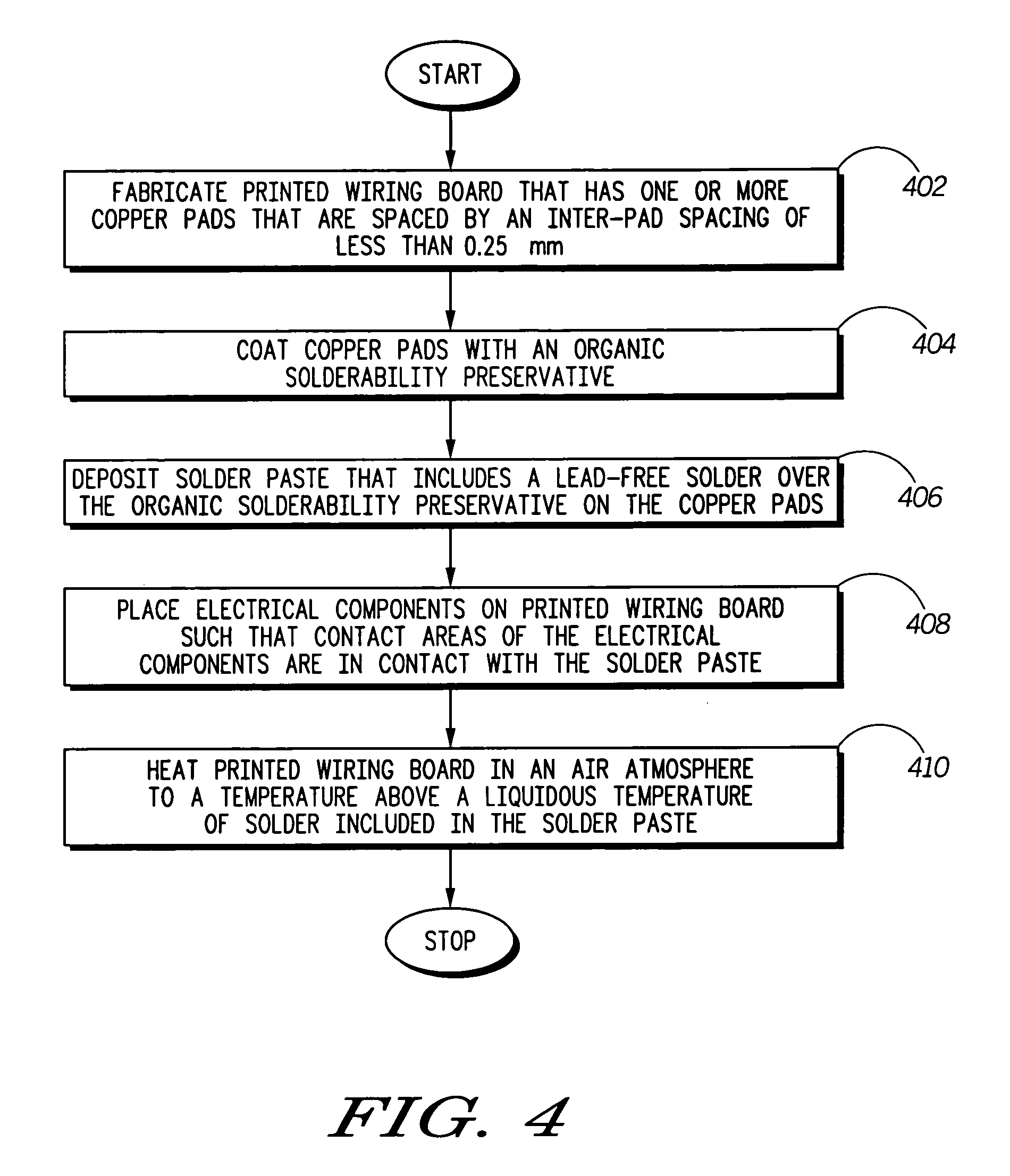
[0042] A second test circuit board 602 shown in FIGS. 7-8 was fabricated. The second test PWB included the same arrays of pads as the first test circuit board. Pads of the second test PWB were coated with Entek OSP. A 5 mill (0.127 mm) thick stencil was used to apply a solder paste that included a solder comprising 95.5 tin, 3.8% silver and 0.7% copper, and a RMA solder flux to the pads of the second test PWB. After application of the solder paste, surface mount resistors were placed on the second test PWB. The second PWB was then heated in an air atmosphere, up to a temperature of 235 C. During the heating a temperature above 217 C was maintained for 70 seconds. The second test PWB was then allowed to cool and the state of the solder joints and discrete components was examined. As shown in FIGS. 7-8, no solder bridges formed, and the surface mount resistor stayed in position.

[0043]FIG. 9 is a sectional side view of a cellular telephone 900 incorporating the populated PWB 100 shown...


PUM

PropertyMeasurementUnit
Lengthaaaaaaaaaa
Lengthaaaaaaaaaa
Fractionaaaaaaaaaa

Abstract

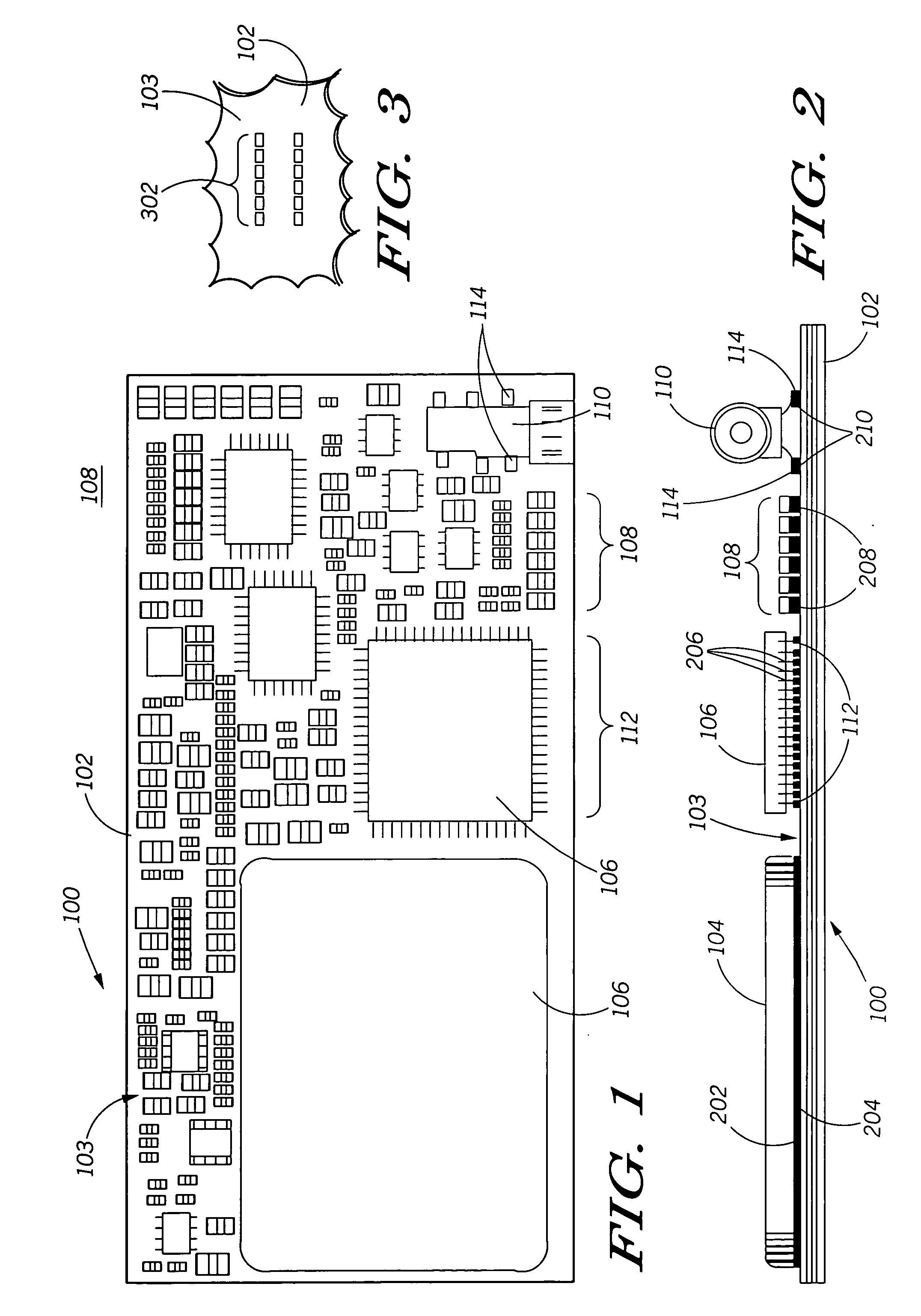
A populated printed wiring board (PWB) (100) and method of manufacturing the populated PWB are taught. The populated PWB is manufactured by fabricating a PWB (102, 402) with exposed copper pads (302), coating the copper pads with an organic solderability preservative (OSP) (404), depositing a solder paste that includes lead-free solder on the OSP covered copper pads (406), placing components (408) and heating the PWB above a liquidous temperature of the lead-free solder in an air atmosphere (410). The process allows very close spacing of components and component leads while forming reliable solder joints to components that are mechanically stressed and components that have non-negligible planarity or coplanarity tolerances.

Description

FIELD OF THE INVENTION [0001] The present invention relates in general to populated printed circuit board manufacturing. More particularly, the present invention relates to printed circuit boards that include very closely spaced pads for, closely spaced components for reduce product size and also include solder joints for components that are mechanically stressed and / or components that have non-negligible planarity or coplanarity tolerances. BACKGROUND OF THE INVENTION [0002] As microelectronic technology has progressed, the degree of circuit integration in microchips has increased to the point that complete electronic devices such as cellular telephones, cameras or handheld computers typically comprise a relatively small number of microchips, along with some discrete components (e.g., resistors, capacitors) connected together on a printed wiring board (PWB). [0003] There are two commonly known types of PWB technologies: the older technology in which component leads are soldered in ...

Claims


Application Information

Patent Timeline
IPC IPC(8): H05K3/28H05K3/34H05K7/06
CPCH05K3/282H05K3/341H05K3/3463Y10T29/5313H05K2201/10189H05K2201/10371H05K2201/10674H05K3/3484H05K3/3485Y02P70/50
Inventor GOUDARZI, VAHID
Owner GOOGLE TECH HLDG LLC
Learn More