Peltier module and manufacturing method therefor
a technology of peltier modules and manufacturing methods, which is applied in the manufacture/treatment of thermoelectric devices, microlithography exposure apparatuses, semiconductor devices, etc., can solve the problems of limiting the overall area for installing thermoelectric semiconductor elements in the peltier module, and it is difficult to produce a high-performance peltier module b>1/b> capable of transferring a relatively large amount of heat, etc., to achieve the effect of increasing the overall sectional area o
- Summary
- Abstract
- Description
- Claims
- Application Information
AI Technical Summary
Benefits of technology
Problems solved by technology
Method used
Image

Examples
first embodiment
1. First Embodiment
[0086] Next, test results regarding the performance of a Peltier module according to a first embodiment of the invention will be described.
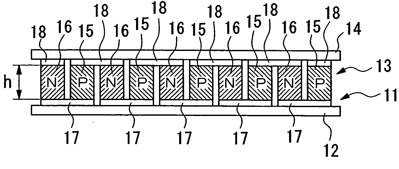
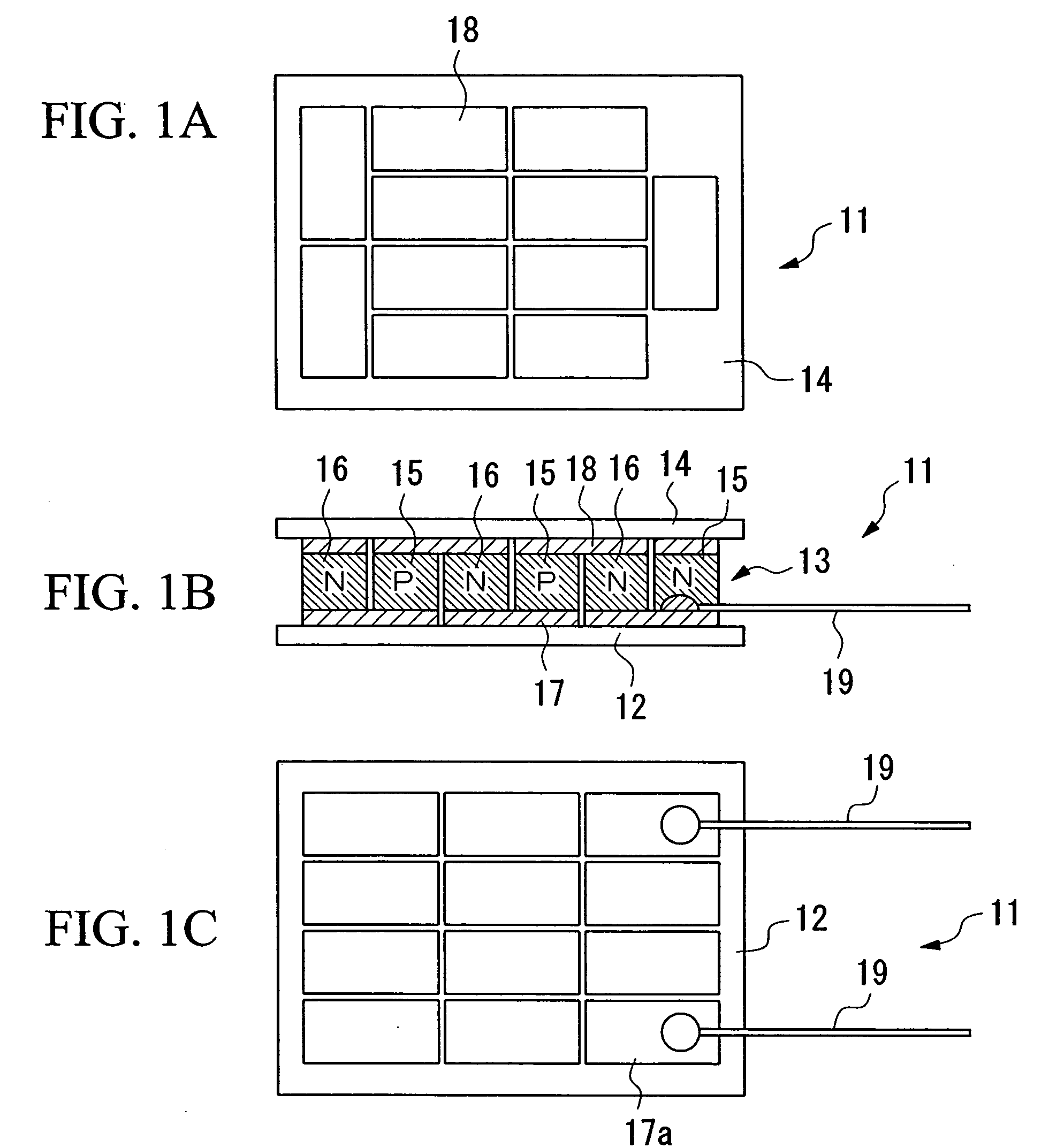
[0087]FIGS. 4 and 5 show the Peltier module 11 according to the first embodiment, which is used in testing and whose dimensions and specifications are shown in Table 1. In the Peltier module 11, both of the substrates 12 and 14 have the same rectangular shape having side lengths a1 and a2. In addition, an electrode-substrate peripheral margin d defines the distance between the peripheral end of the substrate 12 and the peripheral end of the copper electrode 17 arranged in the outmost position within the substrate 12 as well as the distance between the peripheral ends of the substrate 14 and the peripheral end of the copper electrode 18 arranged in the outmost position within the substrate 14; a chip height h defines the height of the P-type thermoelectric semiconductor element 15 and the height of the N-type thermoelectric sem...
second embodiment
2. Second Embodiment
[0095] Next, test results regarding the performance of a large-size Peltier module according to a second embodiment of the invention will be described.
[0096]FIGS. 10 and 11 show the Peltier module 11 of the second embodiment which is subjected to testing and whose dimensions and specifications are shown in Table 2, wherein all values regarding the side lengths a1 and a2 of the substrate 12 (or 14), electrode-substrate peripheral margin d, chip height h, and chip-electrode margin t are set identical to those of the first embodiment shown in Table 1.
TABLE 2Substrate Size a1 × a240 mm × 40 mmSubstrate Peripheral Margin d860 μmChip Height h0.81 mmNumber of Electrodes on Substrate98(Number of P-type or N-type(Total 194 elements)thermoelectric semiconductor elements)Initial Temperature at Substrate 1227° C.Initial Temperature at Substrate 1427° C.Electrode Height D160 μmInter-Electrode Space S50 μm, 100 μm, 200 μm, 500 μmChip-Electrode Margin t10 μm, 20 μm, 50 μm
[00...
third embodiment
3. Third Embodiment
[0103] Next, test results regarding the performance of a small-size Peltier module according to a third embodiment of the invention will be described.
[0104]FIGS. 16 and 17 show the Peltier module 11 of the third embodiment which is subjected to testing and whose dimensions and specifications are shown in Table 3, wherein all values regarding the side lengths a1 and a2 of the substrate 12 (or 14), electrode-substrate peripheral margin d, chip height h, and chip-electrode margin t are set identical to those of the first and second embodiments.
TABLE 3Substrate Size a1 × a21.2 mm × 1.2 mmSubstrate Peripheral Margin d50 μmChip Height h0.31 mmNumber of Electrodes on Substrate6(Number of P-type or N-type(Total 10 elements)thermoelectric semiconductor elements)Initial Temperature at Substrate 1227° C.Initial Temperature at Substrate 1427° C.Electrode Height D50 μmInter-Electrode Space S10 μm, 20 μm, 50 μm, 100 μmChip-Electrode Margin t10 μm, 20 μm, 50 μm
[0105]FIG. 18 i...
PUM
| Property | Measurement | Unit |
|---|---|---|
| aspect ratio D/S | aaaaa | aaaaa |
| thickness | aaaaa | aaaaa |
| viscosity | aaaaa | aaaaa |
Abstract
Description
Claims
Application Information
 - R&D
- Intellectual Property
- Life Sciences
- Materials
- Tech Scout
- Unparalleled Data Quality
- Higher Quality Content
- 60% Fewer Hallucinations
Browse by: Latest US Patents, China's latest patents, Technical Efficacy Thesaurus, Application Domain, Technology Topic, Popular Technical Reports.
© 2025 PatSnap. All rights reserved.Legal|Privacy policy|Modern Slavery Act Transparency Statement|Sitemap|About US| Contact US: help@patsnap.com