System and method for variable array architecture for memories

a memory and array technology, applied in the field of memory circuits, can solve the problems of increasing the density and speed at which dram arrays operate, the potential cost of higher power consumption within a chip, and the inefficient utilization of full chip resources, so as to improve improve the efficiency of memory devices, and reduce the overall power consumption of the operation.

Inactive Publication Date: 2005-06-30
IBM CORP +1
View PDF12 Cites 1 Cited by
  • Summary
  • Abstract
  • Description
  • Claims
  • Application Information

AI Technical Summary

Benefits of technology

[0008] The present invention relates to structures and architecture that improve memory devices. In particular, a design architecture is disclosed that employs simultaneous activation of at least two dissimilar arrays, during a read or write operation. An exemplary embodiment of the current invention includes a memory system containing a plurality of arrays, each in communication with a common controller, wherein the distinguishing feature between arrays is the supply voltage (Vdd). When a microprocessor sends a command to retrieve or write data to the memory system, two or more arrays are addressed to supply the required data. At least two arrays are powered by differing voltages. The faster array(s) (higher Vdd) operate to provide an initial portion of the data, while the array(s) powered by low Vdd, operating less rapidly, provide a complementary portion of the data subsequent to the initial portion. By using arrays of differing Vdd in combination, the requested data is provided in an efficient manner, in which the potential delayed response of the slower, low Vdd, arrays is masked. In an exemplary embodiment this is accomplished by arranging a shorter signal path between the slower array(s) and a memory controller, such that the first group of requested data from the faster, high Vdd, arrays and the second group of data from the low Vdd arrays arrives at the memory controller at about the same time. The overall power consumption of the operation is reduced from what would be required if the data were all resident in high Vdd arrays, without slowing down the operation time, since only the last-required data is retrieved from the slow array(s).

Problems solved by technology

However, these benefits may incur the potential cost of higher power consumption within a chip, as well as inefficient utilization of the full chip resources.
In dynamic random access memory (DRAM) data is accessed and stored in rectangular or square arrays of memory “cells.” Miniaturization has increased both the density and speed at which DRAM arrays operate, often at the expense of increased power consumption.
However, for the same array size, this requires longer wordlines, which requires more cells to be activated during a read or write operation, since all of the cells in a given row must be accessed during such operations.
This, in turn, leads to a longer latency period when a row is being activated.
The operation speed of the memory system may be increased by increasing the supply voltage, but this results in greater power consumption.
Thus, in conventional memory architecture, improvement of one memory feature often results in an adverse impact on another feature.

Method used


Image

  • System and method for variable array architecture for memories
  • System and method for variable array architecture for memories
  • System and method for variable array architecture for memories

Examples


Embodiment Construction

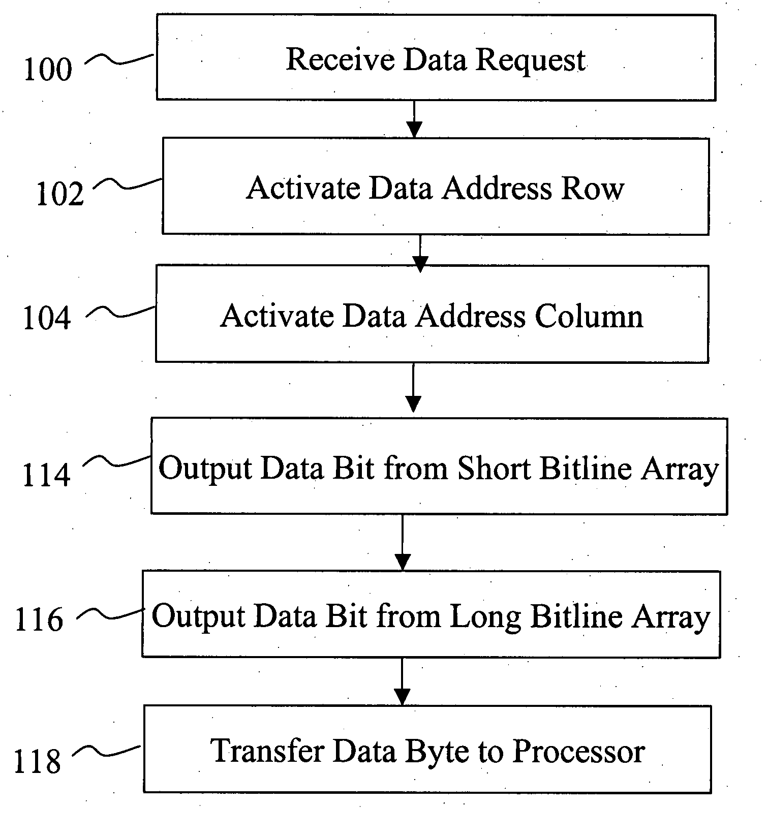
[0023] Before one or more embodiments of the invention are described in detail, one skilled in the art will appreciate that the invention is not limited in its application to the details of construction, the arrangements of components, and the arrangement of steps set forth in the following detailed description or illustrated in the drawings. The invention is capable of other embodiments and of being practiced or being carried out in various ways. For instance, although embodiments disclosed below describe data read operations, embodiments including data write operations are anticipated. In addition, although embodiments refer to manipulation of bits and bytes of data, embodiments employing units of data of a large range of sizes are anticipated. Also, it is to be understood that the phraseology and terminology used herein is for the purpose of description and should not be regarded as limiting.

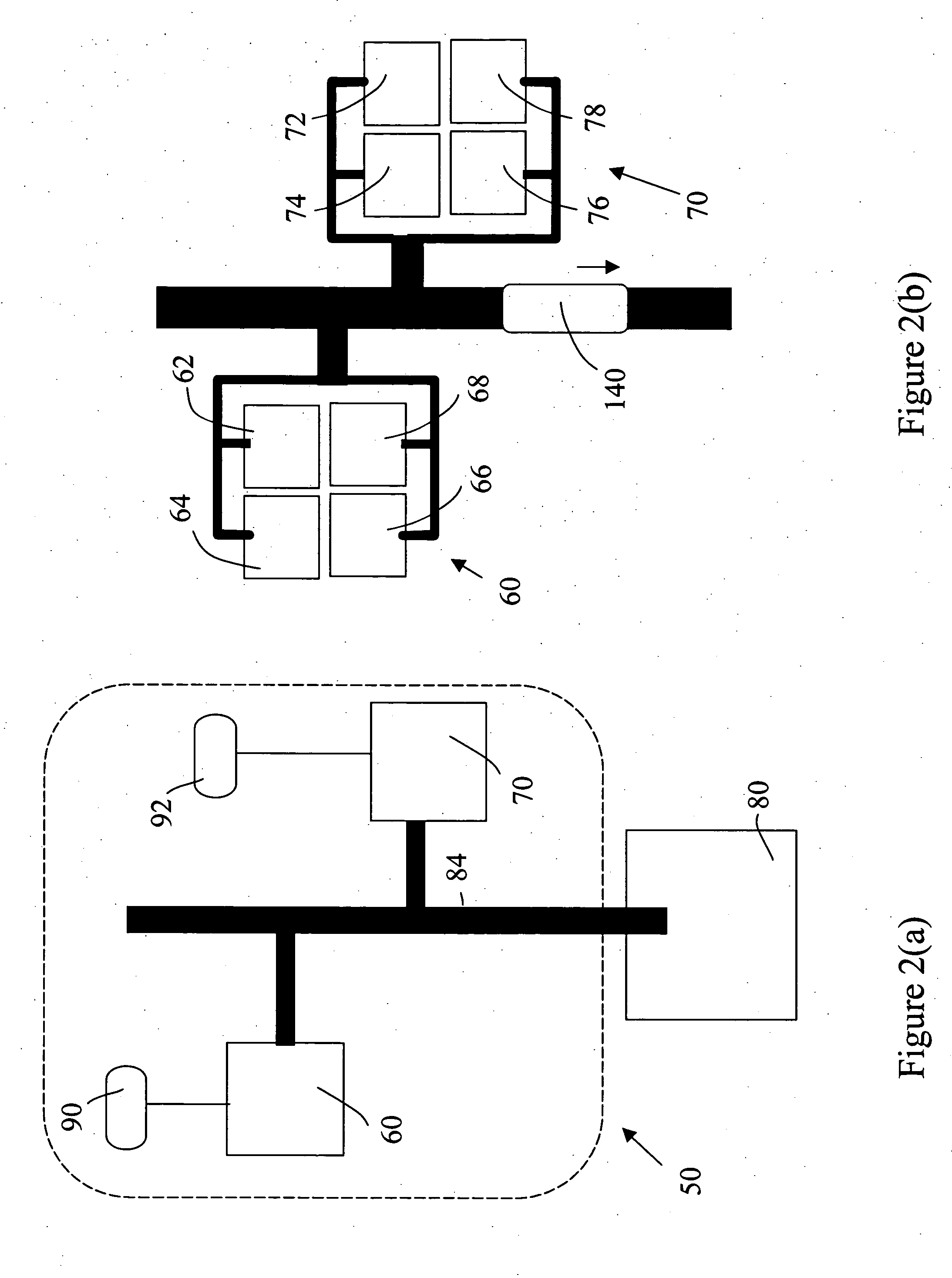
[0024]FIG. 2(a) illustrates a memory system 50, arranged according to an exemplary embod...


PUM


Abstract

A memory system that employs simultaneous activation of at least two dissimilar memory arrays, during a data manipulation, such as read or write operations is disclosed. An exemplary embodiment includes a memory system containing a plurality of arrays, each in communication with a common controller, wherein the arrays are activated by different supply voltage (Vdd). When a processor sends a command to retrieve or write data to the memory system, two or more arrays are addressed to supply the required data. By proper partitioning of the data between dissimilar arrays, the efficiency of data reading is improved.

Description

BACKGROUND [0001] 1. Field of the Invention [0002] The present invention relates generally to memory circuits in integrated circuits. More particularly, the present invention relates to systems and methods for improving dynamic random access memory (DRAM) by employing a variable array architecture. [0003] 2. Background [0004] The semiconductor industry continues to be driven by the benefits imparted by miniaturization of integrated circuits that comprise commercial devices such as memory chips, controllers, and microprocessors. The ability to fabricate increasingly smaller devices and circuits affords the possibility of greater speed, higher device density, and cheaper cost for a given performance. However, these benefits may incur the potential cost of higher power consumption within a chip, as well as inefficient utilization of the full chip resources. In memory devices, both enhanced memory capacity and speed are desirable in order to increase overall system performance. In dynam...

Claims


Application Information

Patent Timeline
Patent Type & Authority Applications(United States)
IPC IPC(8): G06F12/00G06F13/16
CPCY02B60/1228G06F13/1694Y02D10/00
Inventor KIRIHATA, TOSHIAKIMUELLER, GERHARDLUK, WING K.
Owner IBM CORP
Why Eureka
Try Eureka