Method for fabricating semiconductor device
- Summary
- Abstract
- Description
- Claims
- Application Information
AI Technical Summary
Benefits of technology
Problems solved by technology
Method used
Image

Examples
first embodiment
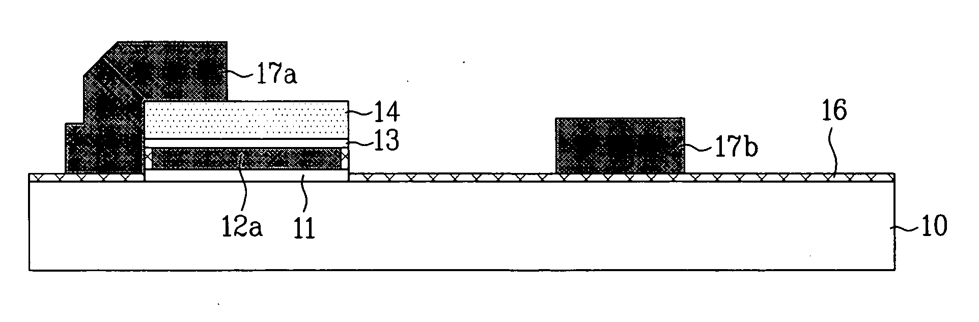
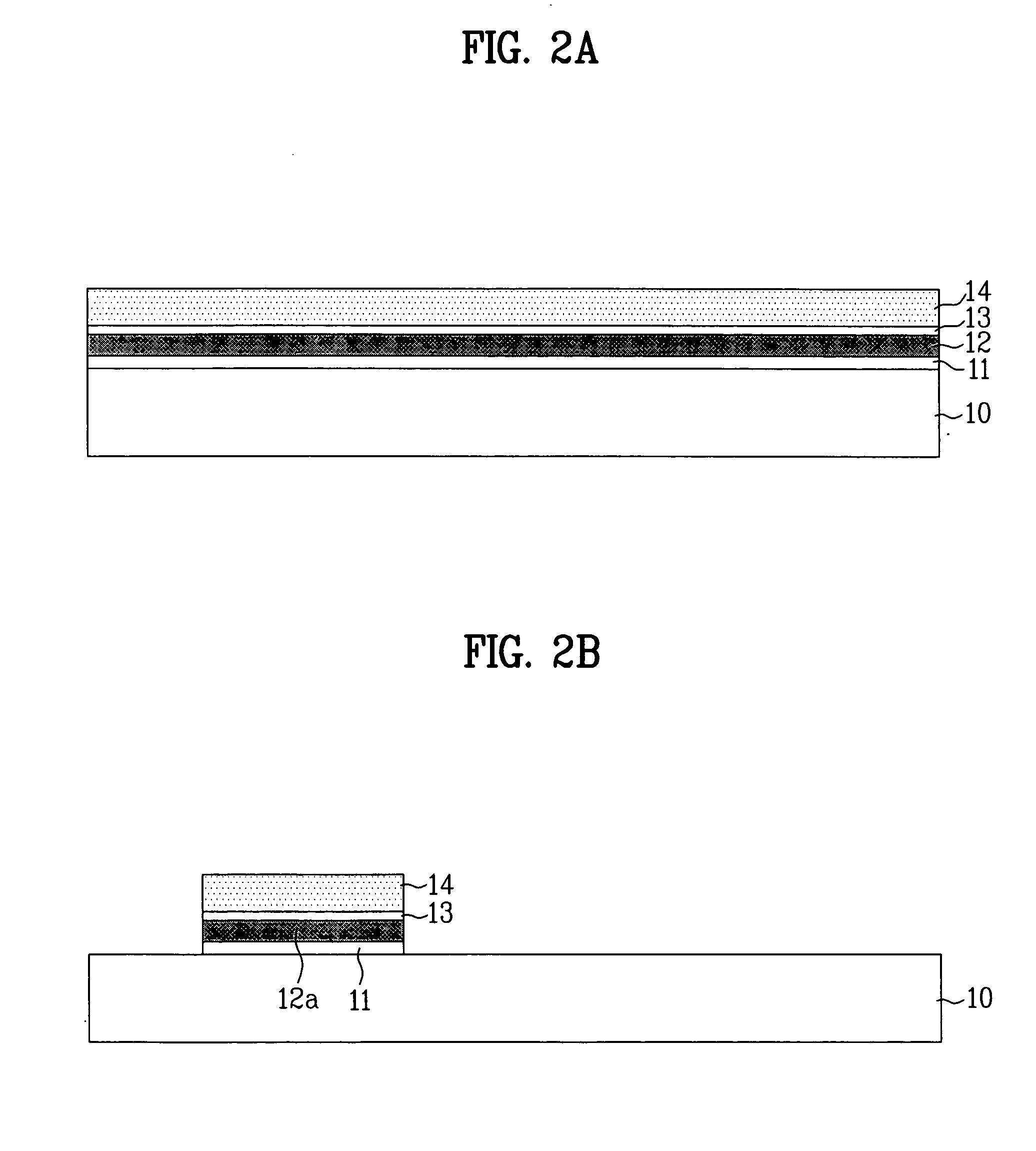
[0044] FIGS. 2A˜2D illustrate sections showing the steps of a method for fabricating a semiconductor device in accordance with a first preferred embodiment of the present invention, and FIG. 3 explains stages of gate oxidation in accordance with a first preferred embodiment of the present invention.
[0045] Referring to FIG. 2A, a first insulating film 11 is formed on a semiconductor substrate 10 having an active cell isolation film formed therein. It is preferable that the first insulating film 11 is an ONO layer having an oxide film having a thickness of 15˜25 Å, a nitride film having a thickness of 90˜110 Å, and an oxide film having a thickness of 30˜50 Å. Then, first polysilicon 12 is deposited on the ONO layer to a thickness of 2000˜3000 Å.
[0046] The first polysilicon is deposited in a state impurity is doped therein, and if the semiconductor substrate 10 is of a P type, polysilicon heavily doped with N type is used. As the N type impurity, there are P or As.
[0047] Then, a sec...
second embodiment
[0056] In the meantime, after removing the impurities diffused from the first polysilicon to the semiconductor substrate by removing the gate oxide film by wet etching, re-oxidation may be performed to form a gate oxide film, which process will be described as follows.
[0057] FIGS. 4A˜4E illustrate sections showing the steps of a method for fabricating a semiconductor device in accordance with a second preferred embodiment of the present invention. FIG. 5 illustrates a graph for comparing threshold voltages of channel regions of transistors formed at a logical circuit region in cases re-oxidation is performed in accordance with a second preferred embodiment of the present invention, and the re-oxidation is not performed.
[0058] Referring to FIG. 4A, a first insulating film 11 is formed on a semiconductor substrate 10 having an active cell isolation film formed therein. It is preferable that the first insulating film 11 is an ONO layer having an oxide film having a thickness of 15˜25...
third embodiment
[0068] In the meantime, by forming a sidewall insulating film at sides of the floating gate pattern, the drop of the threshold voltage of the transistor can be prevented, which will be described in detail, as follows.
[0069] FIGS. 6A˜6E illustrate sections showing the steps of a method for fabricating a semiconductor device in accordance with a third preferred embodiment of the present invention.
[0070] Referring to FIG. 6A, a first insulating film 11 is formed on a semiconductor substrate 10 having an active cell isolation film formed therein. It is preferable that the first insulating film 11 is an ONO layer having an oxide film having a thickness of 15˜25 Å, a nitride film having a thickness of 90˜110 Å, and an oxide film having a thickness of 30˜50 Å. Then, first polysilicon 12 is deposited on the ONO layer to a thickness of 2000˜3000 Å.
[0071] The first polysilicon is deposited in a state impurity is doped therein, and if the semiconductor substrate 10 is of a P type, polysilic...
PUM
 Abstract
Description
Claims
Application Information
 - R&D
- Intellectual Property
- Life Sciences
- Materials
- Tech Scout
- Unparalleled Data Quality
- Higher Quality Content
- 60% Fewer Hallucinations
Browse by: Latest US Patents, China's latest patents, Technical Efficacy Thesaurus, Application Domain, Technology Topic, Popular Technical Reports.
© 2025 PatSnap. All rights reserved.Legal|Privacy policy|Modern Slavery Act Transparency Statement|Sitemap|About US| Contact US: help@patsnap.com