Delay circuit and display including the same

a delay circuit and display technology, applied in the field of delay circuits and displays, can solve the problems of increasing the time delay of output signals in delay circuits, and achieve the effect of suppressing the reduction of manufacturing yield

Inactive Publication Date: 2005-06-30
SANYO ELECTRIC CO LTD
View PDF10 Cites 2 Cited by
  • Summary
  • Abstract
  • Description
  • Claims
  • Application Information

AI Technical Summary

Benefits of technology

[0017] The present invention has been proposed in order to provide a delay circuit capable of suppressing reduction of the yield in manufacturing.
[0018] The present invention has also been proposed in order to provide a display including a delay circuit capable of suppressing reduction of the yield in manufacturing.
[0020] The delay circuit according to the first aspect can increase the time for bringing the input signal in the inverter circuit from the first voltage to the voltage corresponding to the logical threshold voltage of the inverter circuit due to the action of the first transistor functioning substantially as a capacitor. Thus, the delay circuit can increase the time delay of the output signal at the time when the input signal in the inverter circuit changes from the first voltage to the second voltage without extremely increasing the ratio between the gate widths of transistors constituting the inverter circuit dissimilarly to the conventional delay circuit. Therefore, the delay circuit can increase the time delay of the output signal at the time when the input signal in the inverter circuit changes from the first voltage to the second voltage without extremely reducing the gate widths of the transistors constituting the inverter circuit, whereby the yield can be inhibited from reduction in formation of the delay circuit.
[0022] The display including a delay circuit according to the second aspect can increase the time for bringing the input signal in the inverter circuit from the first voltage to the voltage corresponding to the logical threshold voltage of the inverter circuit due to the action of the first transistor functioning substantially as a capacitor. Thus, the display can increase the time delay of the output signal at the time when the input signal in the inverter circuit changes from the first voltage to the second voltage without extremely increasing the ratio between the gate widths of transistors constituting the inverter circuit dissimilarly to the conventional delay circuit. Therefore, the display can increase the time delay of the output signal at the time when the input signal in the inverter circuit changes from the first voltage to the second voltage without extremely reducing the gate widths of the transistors constituting the inverter circuit, whereby the yield can be inhibited from reduction in formation of the delay circuit. Consequently, the yield can be inhibited from reduction in formation of the display including the delay circuit.

Problems solved by technology

Thus, the delay circuit can increase the time delay of the output signal at the time when the input signal in the inverter circuit changes from the first voltage to the second voltage without extremely increasing the ratio between the gate widths of transistors constituting the inverter circuit dissimilarly to the conventional delay circuit.

Method used


Image

  • Delay circuit and display including the same
  • Delay circuit and display including the same
  • Delay circuit and display including the same

Examples


Embodiment Construction

[0036] An embodiment of the present invention is now described with reference to FIGS. 1 to 11.

[0037] First, the structures of delay circuits and a display 50 including the same according to this embodiment are described with reference to FIGS. 1 to 6.

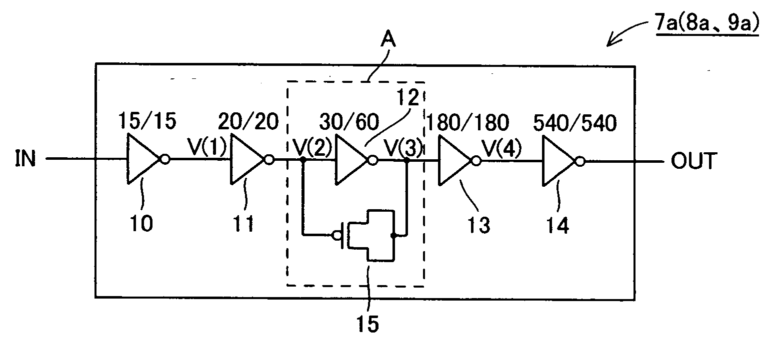
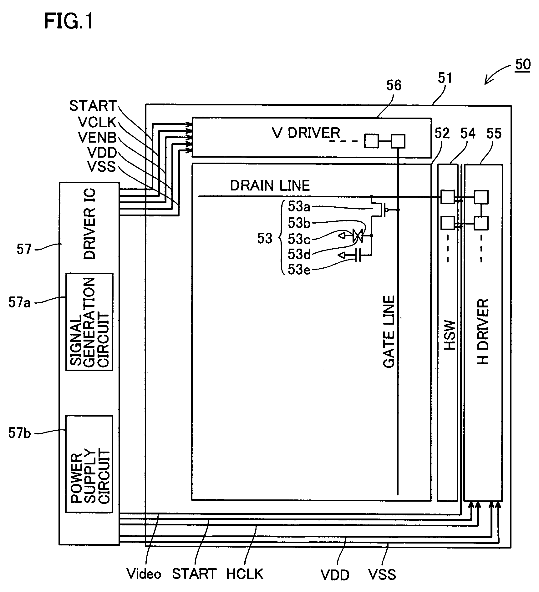
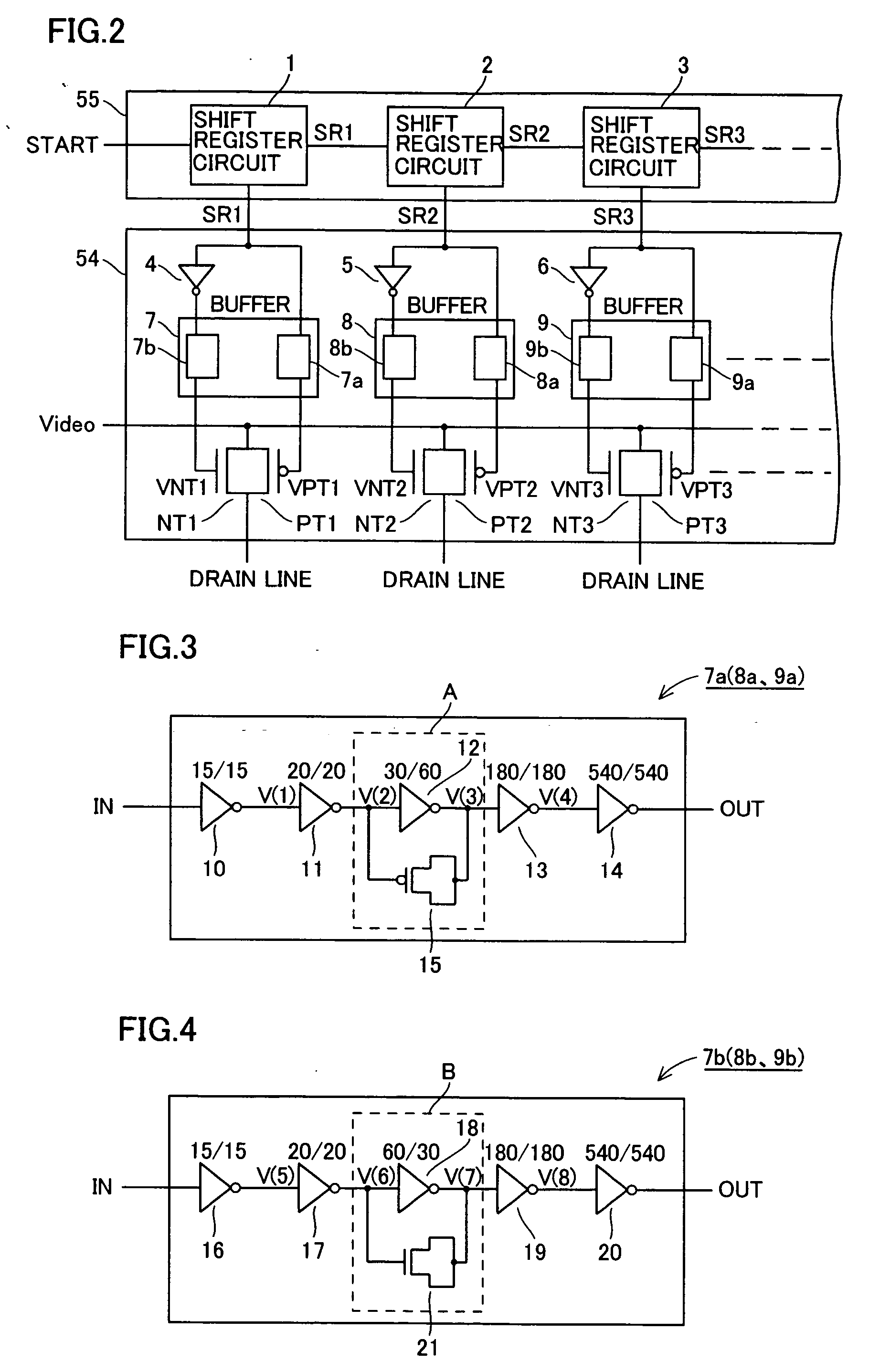
[0038] In the display 50 including delay circuits according to this embodiment, an image display portion 52 is provided on a substrate 51, as shown in FIG. 1. Pixels 53 are arranged on the image display portion 52 in the form of a matrix. FIG. 1 shows the structure of only one pixel 53 of the image display portion 52. Each pixel 53 is constituted of a p-channel transistor 53a, a pixel electrode 53b, a common electrode 53c, common to the respective pixels 53, arranged oppositely to the pixel electrode 53b, a liquid crystal 53b held between the pixel electrode 53b and the common electrode 53c and a subsidiary capacitance 53e. The p-channel transistor 53a has a source connected to a drain line, a drain connected to the pixel electrode 5...


PUM


Abstract

A delay circuit capable of suppressing reduction of the yield in manufacturing is provided. This delay circuit comprises an inverter circuit having a prescribed logical threshold voltage and a first transistor connected in parallel to the inverter circuit. The first transistor is turned on when an input signal in and an output signal from the inverter circuit are at a first voltage and a second voltage respectively and further turned on for at least a partial period in a period when the input signal in the inverter circuit reaches a voltage corresponding to the logical threshold voltage of the inverter circuit from the first voltage for changing from the first voltage to the second voltage thereby functioning substantially as a capacitor.

Description

BACKGROUND OF THE INVENTION FIELD OF THE INVENTION [0001] The present invention relates to a delay circuit and a display including the same, and more particularly, it relates to a delay circuit employing an inverter circuit and a display including the same. CROSS-REFERENCE TO RELATED APPLICATIONS The priority application number JP2003-426879 upon which this patent application is based is hereby incorporated by reference. DESCRIPTION OF THE BACKGROUND ART [0002] In general, a delay circuit employing an inverter circuit is known as disclosed in Japanese Patent Laying-Open No. 5-14152 (1993), for example. The aforementioned Japanese Patent Laying-Open No. 5-14152 discloses a delay circuit formed by serially connecting a plurality of inverter circuits with each other. [0003]FIG. 12 is a circuit diagram for illustrating the structure of a display including delay circuits similar to that disclosed in the aforementioned Japanese Patent Laying-Open No. 5-14152. FIGS. 13 and 14 are circuit d...

Claims


Application Information

Patent Timeline
Patent Type & Authority Applications(United States)
IPC IPC(8): G09G3/20G09G3/36H03K5/00H03K5/13H03K5/153H03K17/28H03K17/687H03K19/096
CPCG09G3/3688H03K2005/00156H03K5/133G09G2310/0294H03K5/14G09G3/36
Inventor SENDA, MICHIRU
Owner SANYO ELECTRIC CO LTD
Why Eureka
Try Eureka