Display device, inspection method for display device, and inspection device for display device

a display device and display device technology, applied in static indicating devices, individual semiconductor device testing, instruments, etc., can solve the problems of reducing manufacturing yield, mounting expensive components, and not being able to inspect wiring defects in each of the wiring line groups, etc., to achieve the effect of suppressing the decrease in manufacturing yield

Active Publication Date: 2010-09-14
JAPAN DISPLAY CENTRAL CO LTD
View PDF11 Cites 2 Cited by
  • Summary
  • Abstract
  • Description
  • Claims
  • Application Information

AI Technical Summary

Benefits of technology

[0009]The present invention has been made in consideration of the above-described problems, and the object of the invention is to provide a display device, an inspection method for a display device, and an inspection device for a display device, which can exactly detect a wiring defect on a panel and can suppress a decrease in manufacturing yield.
[0015]The present invention can provide a display device, an inspection method for a display device, and an inspection device for a display device, which can exactly detect a wiring defect on a panel and can suppress a decrease in manufacturing yield.

Problems solved by technology

However, it is not possible to inspect a wiring defect in each of the wiring line groups.
In the subsequent fabrication step, expensive components, as a driving IC chip and a flexible print circuit board (FPC), are mounted.
Thus, if the defective panel goes to the subsequent fabrication step, this leads to a decrease in manufacturing yield.

Method used


Image

  • Display device, inspection method for display device, and inspection device for display device
  • Display device, inspection method for display device, and inspection device for display device
  • Display device, inspection method for display device, and inspection device for display device

Examples


first embodiment

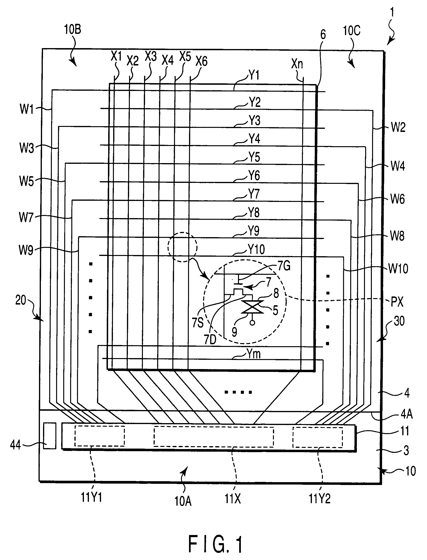
[0028]As is shown in FIG. 1, a liquid crystal display device, which is an example of a display device according to a first embodiment, includes a substantially rectangular, planar liquid crystal display panel 1. The liquid crystal display panel 1 comprises a pair of substrates, that is, an array substrate 3 and a counter-substrate 4, and a liquid crystal layer 5 that is interposed as an optical modulation layer between the pair of substrates. The liquid crystal display panel 1 includes a substantially rectangular effective display section 6 that displays an image. The effective display section 6 is composed of a plurality of display pixels PX that are arranged in a matrix.

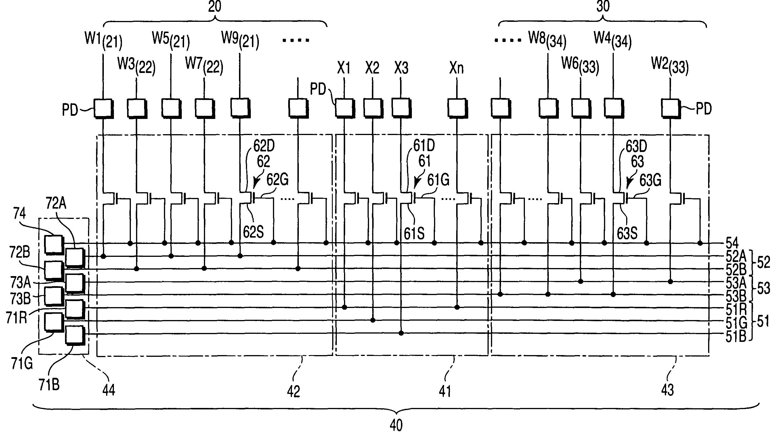
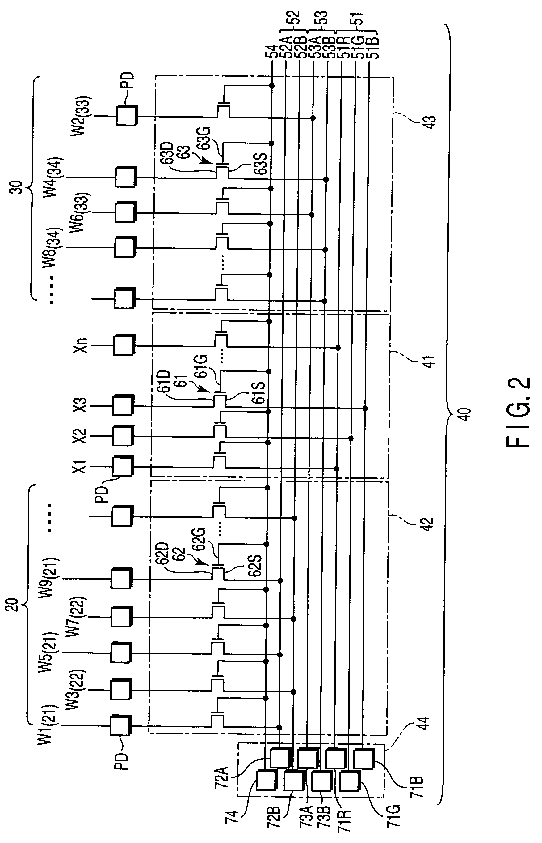
[0029]The array substrate 3 includes, in the effective display section 6, a plurality of scan lines Y (1, 2, 3, . . . , m) that extend in a row direction of the display pixels PX, a plurality of signal lines X (1, 2, 3, . . . , n) that extend in a column direction of the display pixels PX, switching elements 7 that...

second embodiment

[0084]In the description of a second embodiment of the invention, the structural elements that are common to those in the first embodiment are denoted by like reference numerals.

[0085]As is shown in FIG. 6, a liquid crystal display device, which is an example of a display device according to the second embodiment, includes a substantially rectangular, planar liquid crystal display panel, that is, a main panel 1. The main panel 1 comprises a pair of substrates, that is, an array substrate 3 and a counter-substrate 4, and a liquid crystal layer 5 that is interposed as an optical modulation layer between the pair of substrates. The main panel 1 includes a rectangular first effective display section 6A that displays an image. The first effective display section 6A is composed of a plurality of display pixels PX that are arranged in a matrix.

[0086]The array substrate 3 includes a plurality of scan lines MY (1, 2, 3, . . . , m) that extend in a row direction of the display pixels PX, a pl...


PUM

PropertyMeasurementUnit
areaaaaaaaaaaa
defectaaaaaaaaaa
flexibleaaaaaaaaaa

Abstract

A display device includes a first wiring line group of wiring lines connected to odd-number-th scan lines, a second wiring line group of wiring lines connected to even-number-th scan lines, a first inspection wiring line connected to first wiring lines of the first wiring line group, a second inspection wiring line connected to second wiring lines of the first wiring line group, which neighbor the first wiring lines, a third inspection wiring line connected to third wiring lines of the second wiring line group, and a fourth inspection wiring line connected to fourth wiring lines of the second wiring line group, which neighbor the third wiring lines.

Description

CROSS-REFERENCE TO RELATED APPLICATIONS[0001]This application is based upon and claims the benefit of priority from prior Japanese Patent Applications No. 2004-231107, filed Aug. 6, 2004; and No. 2004-231110, filed Aug. 6, 2004, the entire contents of both of which are incorporated herein by reference.BACKGROUND OF THE INVENTION[0002]1. Field of the Invention[0003]The present invention relates to a display device that includes inspection wiring lines for inspecting a wiring defect, an inspection method for inspecting a wiring defect on the basis of inspection signals that are input to the inspection wiring lines of the display device, and an inspection device that generates inspection signals, which are input to the inspection wiring lines of the display device.[0004]2. Description of the Related Art[0005]A display device, such as a liquid crystal display device, includes an effective display section that is composed of display pixels arranged in a matrix. The effective display devi...

Claims


Application Information

Patent Timeline
Patent Type & Authority Patents(United States)
IPC IPC(8): G02F1/133
CPCG09G3/006G09G3/3648G06F3/1423G09G3/3666G09G2300/0426G09G2310/0218G09G2310/0278G09G2330/12G02F1/1345
Inventor KIMURA, YOHEINAKAYAMA, KOJIHARADA, KAZUYUKI
Owner JAPAN DISPLAY CENTRAL CO LTD
Why Eureka
Try Eureka