Array substrate for display device

a display device and substrate technology, applied in the direction of electrical equipment, semiconductor devices, radio frequency controlled devices, etc., can solve the problems of deterioration in manufacturing yield, voids, foreign matter dissolving, etc., and achieve the effect of suppressing deterioration in optical characteristics and suppressing a decrease in manufacturing yield

Inactive Publication Date: 2008-09-02
JAPAN DISPLAY CENTRAL CO LTD
View PDF2 Cites 4 Cited by
  • Summary
  • Abstract
  • Description
  • Claims
  • Application Information

AI Technical Summary

Benefits of technology

[0009]The present invention has been made in consideration of the above-described problem, and the object of the invention is to provide an array substrate for a display device which can suppress a decrease in manufacturing yield while suppressing deterioration in optical characteristics.
[0011]The present invention can provide an array substrate for a display device which can suppress a decrease in manufacturing yield while suppressing deterioration in optical characteristics.

Problems solved by technology

In particular, in the case where hydrogen fluoride (HF) is used as a cleaning agent, foreign matter is dissolved and a void occurs.
In worst cases, even the insulating substrate is etched, leading to deterioration in manufacturing yield.
In the case where a semiconductor layer with a thickness of about 50 nm is disposed on the undercoat layer, if foreign matter of a sub-micron level is present, it is difficult to completely cover the foreign matter with these films.
In addition, if the thicknesses of the silicon nitride film and silicon oxide film are simply increased, deterioration may occur in optical characteristics of the display device, such as transmittance and chromaticity.
Thus, the thicknesses of these films are set in a limited range.

Method used


Image

  • Array substrate for display device
  • Array substrate for display device
  • Array substrate for display device

Examples


Embodiment Construction

[0019]An array substrate for a display device according to an embodiment of the present invention is described with reference to the accompanying drawings.

[0020]To begin with, the structure of the array substrate according to the embodiment is described. The structure of the array substrate, which is applied to a liquid crystal display device as an active-matrix flat-panel display device, is described.

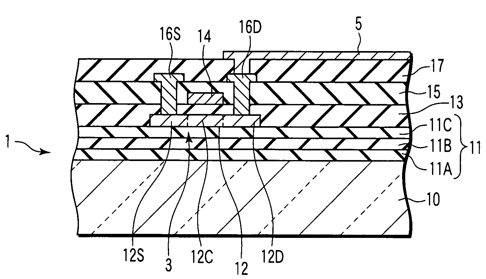
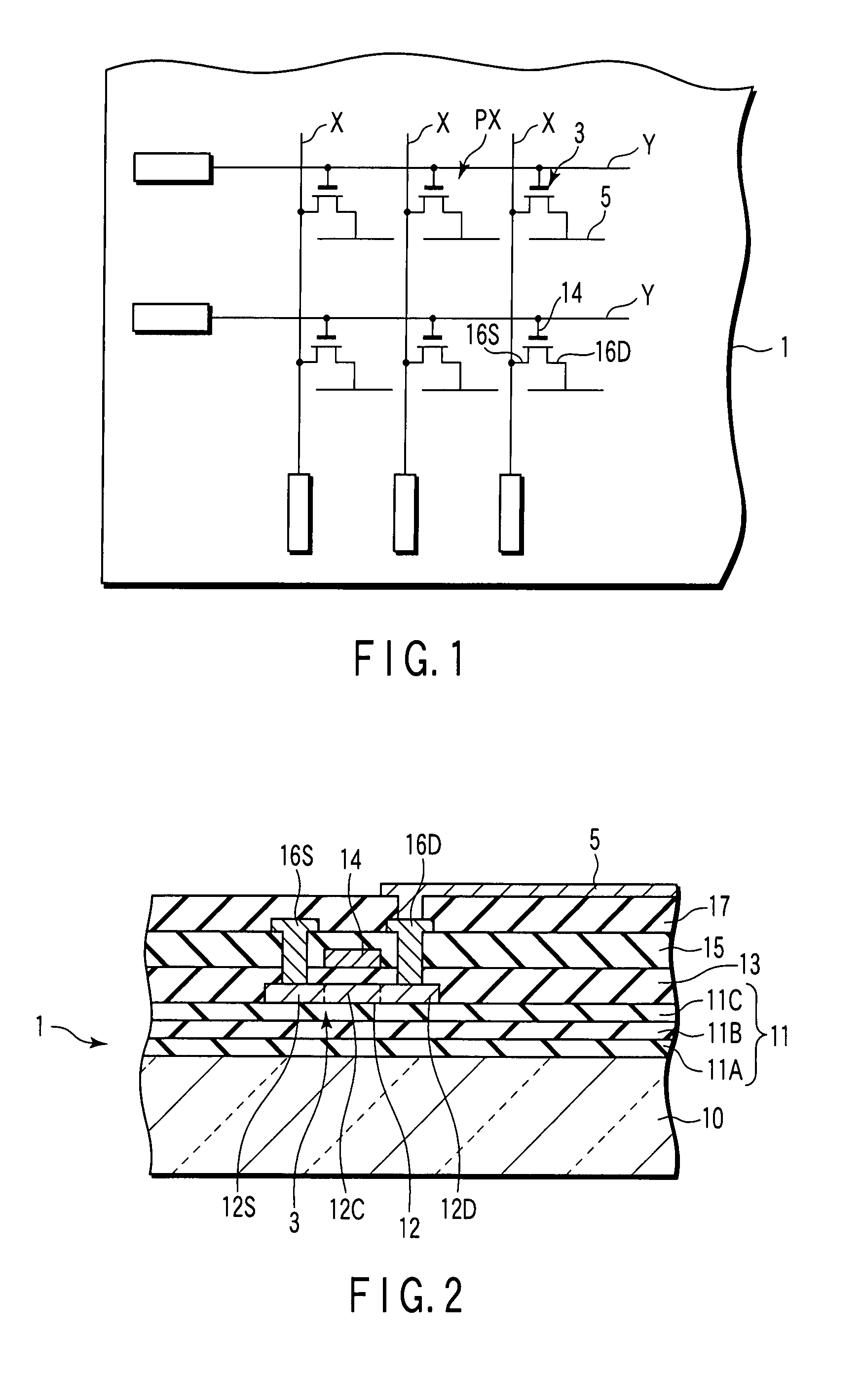
[0021]As is shown in FIG. 1, an array substrate 1 includes a plurality of pixels PX which are arrayed in a matrix. The array substrate 1 includes a plurality of scanning lines Y, which extend in a row direction of the pixels PX, and a plurality of signal lines X which extend in a column direction of the pixels PX. The scanning lines Y and signal lines X are arranged via an insulation layer and are mutually insulated. The array substrate 1 includes switching elements 3, which are disposed in the respective pixels PX in regions including intersections between the scanning lines Y and sig...


PUM


Abstract

An array substrate for a display device includes an insulating substrate, a buffer layer which is disposed on the insulating substrate and is formed of silicon oxide with a refractive index equal to a refractive index of the insulating substrate, a first insulation layer which is disposed on the buffer layer and formed of silicon nitride, a second insulation layer which is disposed on the first insulation layer and formed of silicon oxide, a switching element including a semiconductor layer disposed on the second insulation layer, and a pixel electrode connected to the switching element.

Description

CROSS-REFERENCE TO RELATED APPLICATIONS[0001]This application is based upon and claims the benefit of priority from prior Japanese Patent Application No. 2006-074584, filed Mar. 17, 2006, the entire contents of which are incorporated herein by reference.BACKGROUND OF THE INVENTION[0002]1. Field of the Invention[0003]The present invention relates generally to an array substrate for a display device, and more particularly to the structure of an undercoat layer between an insulating substrate and a semiconductor layer.[0004]2. Description of the Related Art[0005]An array substrate, which is applied to an active-matrix flat-panel display device such as a liquid crystal display device or an organic electroluminescence display device, includes switching elements which are disposed in matrix-arrayed pixels. For example, in a case where a top-gate type thin-film transistor, which includes a semiconductor layer formed of amorphous silicon or polysilicon, is applied to the switching element, ...

Claims


Application Information

Patent Timeline
Patent Type & Authority Patents(United States)
IPC IPC(8): H01L29/15
CPCH01L27/12H01L29/78603
Inventor ADACHI, NORIYUKI
Owner JAPAN DISPLAY CENTRAL CO LTD
Why Eureka
Try Eureka