Semiconductor nano-wire, making method thereof and semiconductor device provided with that nano-wire
A nanowire and semiconductor technology, applied in the fields of semiconductor/solid-state device manufacturing, semiconductor devices, nanotechnology, etc., can solve the problems of small contact area between nanowires and source/drain electrodes, plastic substrates not resistant to contact resistance reduction heat treatment, etc. , to achieve the effect of simplifying the manufacturing process, low contact resistance, and suppressing the deviation of mask alignment
- Summary
- Abstract
- Description
- Claims
- Application Information
AI Technical Summary
Problems solved by technology
Method used
Image

Examples
Embodiment approach 1
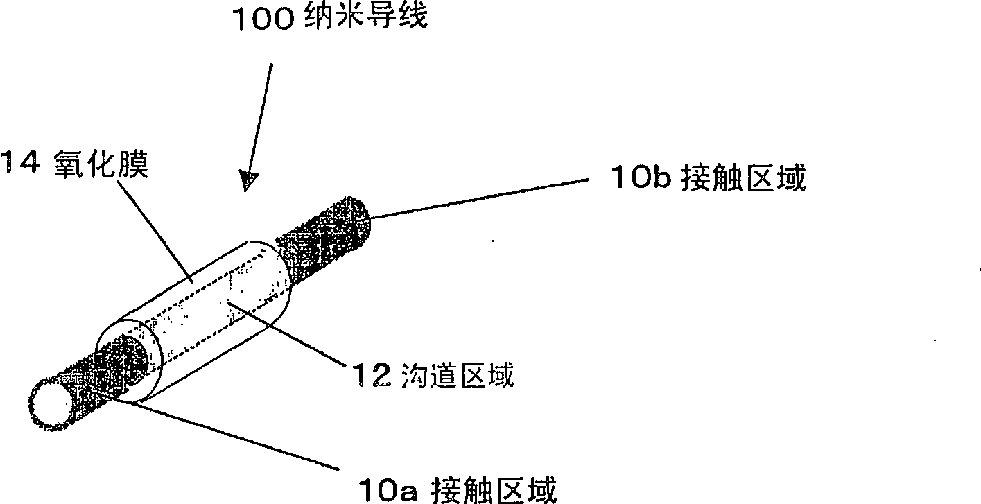
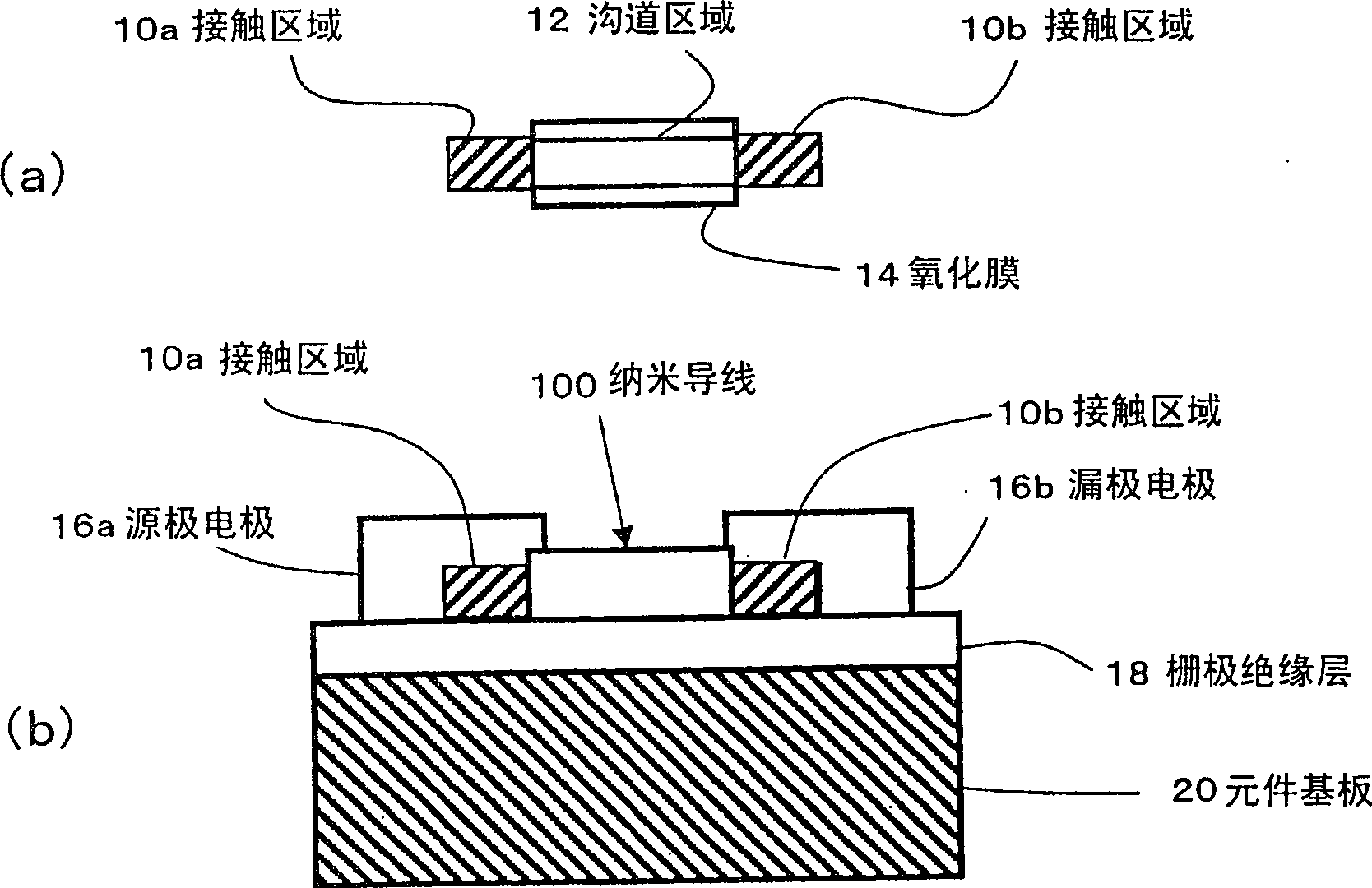
[0061] Below, refer to figure 1 and figure 2 , the first embodiment of the nanowire of the present invention will be described. figure 1 It is a perspective view of the nanowire 100 in this embodiment. figure 2 (a) is a cross-sectional view along the long axis direction of the nanowire 100, figure 2 (b) is a cross-sectional view of a field effect transistor including the nanowire 100 .
[0062] figure 1 and figure 2 The illustrated nanowire 100 has: a pair of contact regions 10a, 10b; and a channel region 12 connected to these contact regions 10a, 10b. In the present embodiment, the channel region 12 is formed of silicon (Si), but the contact regions 10a and 10b have conductive portions formed of a material different from Si at least on the surface. More specifically, the contact regions 10a, 10b are configured to include: a core portion made of Ge doped with a p-type impurity at a high concentration; and an alloy portion (here, The channel region of the p-type semi...
Embodiment approach 2
[0107] Below, refer to Figure 9 (a) and (b) describe the second embodiment of the present invention.
[0108] Figure 9 (a) is a figure which shows the nanowire of this embodiment, Figure 9 (b) is a top view of a field-effect transistor fabricated using this nanowire.
[0109] The characteristic of this embodiment is that, if Figure 9 As shown in (a), a nanowire includes more than 3 contact regions 10 1 ~10 N (N is an integer greater than or equal to 3), two or more channel regions 12 1 ~12 M (M is an integer of 2 or more).
[0110] Such nanowires can be referenced by repeatedly performing Figure 5 The crystal growth processes described in (b) to (d) are produced, for example, by alternately growing Ge portions and Si portions. In this case, only the Si portion is covered with an insulating film, and the surface of the Ge portion is selectively alloyed, as in the above-described embodiment.
[0111] from Figure 9 (b) It can be seen that the "channel length" of ...
Embodiment approach 3
[0125] Below, refer to Figure 11 A third embodiment of the present invention will be described.
[0126] Figure 11 It is a plan view of a field effect transistor produced using the nanowire 200 of this embodiment. and Image 6 The field effect transistor shown differs in that the length of the channel region of the nanowire 200 is shorter than the separation between the source electrode 16a and the drain electrode 16b.
[0127] In this embodiment mode, the channel length is shortened beyond the limit of photolithography technology. As mentioned above, the channel length is defined as the length of the channel region of the nanowire, which can be controlled by the growth process of the nanowire. Therefore, the length of the channel region can be set to an extremely short value (for example, in the range of 50 to 1000 nm, preferably 500 nm or less), regardless of the limit of photolithography technology.
PUM
 Abstract
Description
Claims
Application Information
 - R&D
- Intellectual Property
- Life Sciences
- Materials
- Tech Scout
- Unparalleled Data Quality
- Higher Quality Content
- 60% Fewer Hallucinations
Browse by: Latest US Patents, China's latest patents, Technical Efficacy Thesaurus, Application Domain, Technology Topic, Popular Technical Reports.
© 2025 PatSnap. All rights reserved.Legal|Privacy policy|Modern Slavery Act Transparency Statement|Sitemap|About US| Contact US: help@patsnap.com