Semiconductor circuit device simulation method and semiconductor circuit device simulator
a semiconductor circuit device and simulator technology, applied in the field of semiconductor circuit device simulator and semiconductor circuit device simulator, can solve the problems of significant problems such as deterioration of drain current, significant problems of semiconductor circuit device including mis transistor, etc., and increase the delay time of the circui
- Summary
- Abstract
- Description
- Claims
- Application Information
AI Technical Summary
Benefits of technology
Problems solved by technology
Method used
Image

Examples
first embodiment
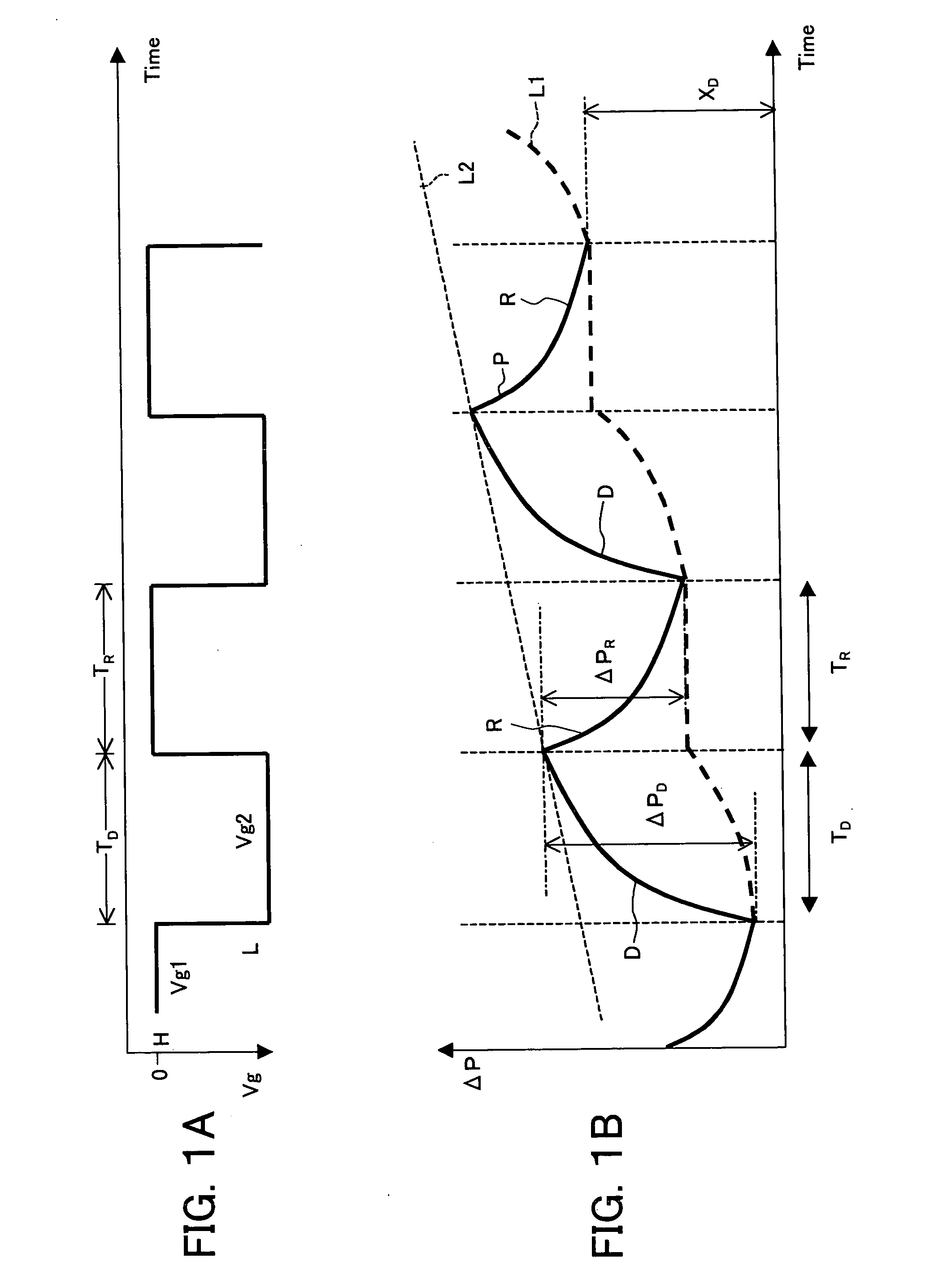
[0104] The present inventors perceived details of the NBTI (Negative Bias Temperature Instability) deterioration phenomenon of a MIS transistor, particularly, a characteristics deterioration phenomenon of a transistor and a recovery phenomenon of a transistor characteristics after characteristics deterioration by experimental data and, based on the experimental data, found an empiric formula expressing the deterioration phenomenon and recovery phenomenon for simulating the NBTI deterioration phenomenon.
[0105]FIG. 1A and FIG. 1B schematically show changes of. transistor characteristics, such as a driving ability and a threshold voltage, over time as the NBTI deterioration phenomenon, and shows an example where the transistor characteristics deteriorate over time due to a gate voltage applied to a gate of the transistor. FIG. 1A shows changes of a pulse waveform of a gate voltage “Vg” over time, and in FIG. 1B, the ordinate axis indicates a total deterioration amount ΔP of any charac...
second embodiment
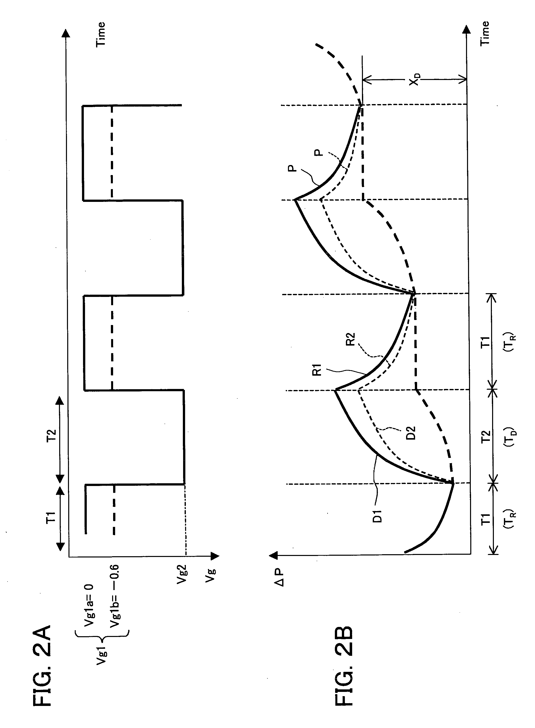
[0178] In the first embodiment, a basic deterioration amount XD(t) was expressed by using the formulas 26 to 29 for a simple description, but the present inventors found to express an actual basic deterioration amount XD(t) by a plurality of different functions in a plurality of time zones and not by one function defined for one time zone as in the conventional way.
[0179]FIG. 4 shows changes of a basic deterioration amount XD(t) over time wherein a conventional calculation method and a calculation method of the present invention are compared for illustration.
[0180] A dotted straight line indicates changes of a basic deterioration amount XD′ over time by a conventional calculation formula, and a solid sequential line indicates a basic deterioration amount by embodiments of the present invention.
[0181] In the embodiments of the present invention, for example in three divided time zones (t1, t12, t2), basic deterioration amounts XD1, XD2 and XD3 in respective time zones are expresse...
third embodiment
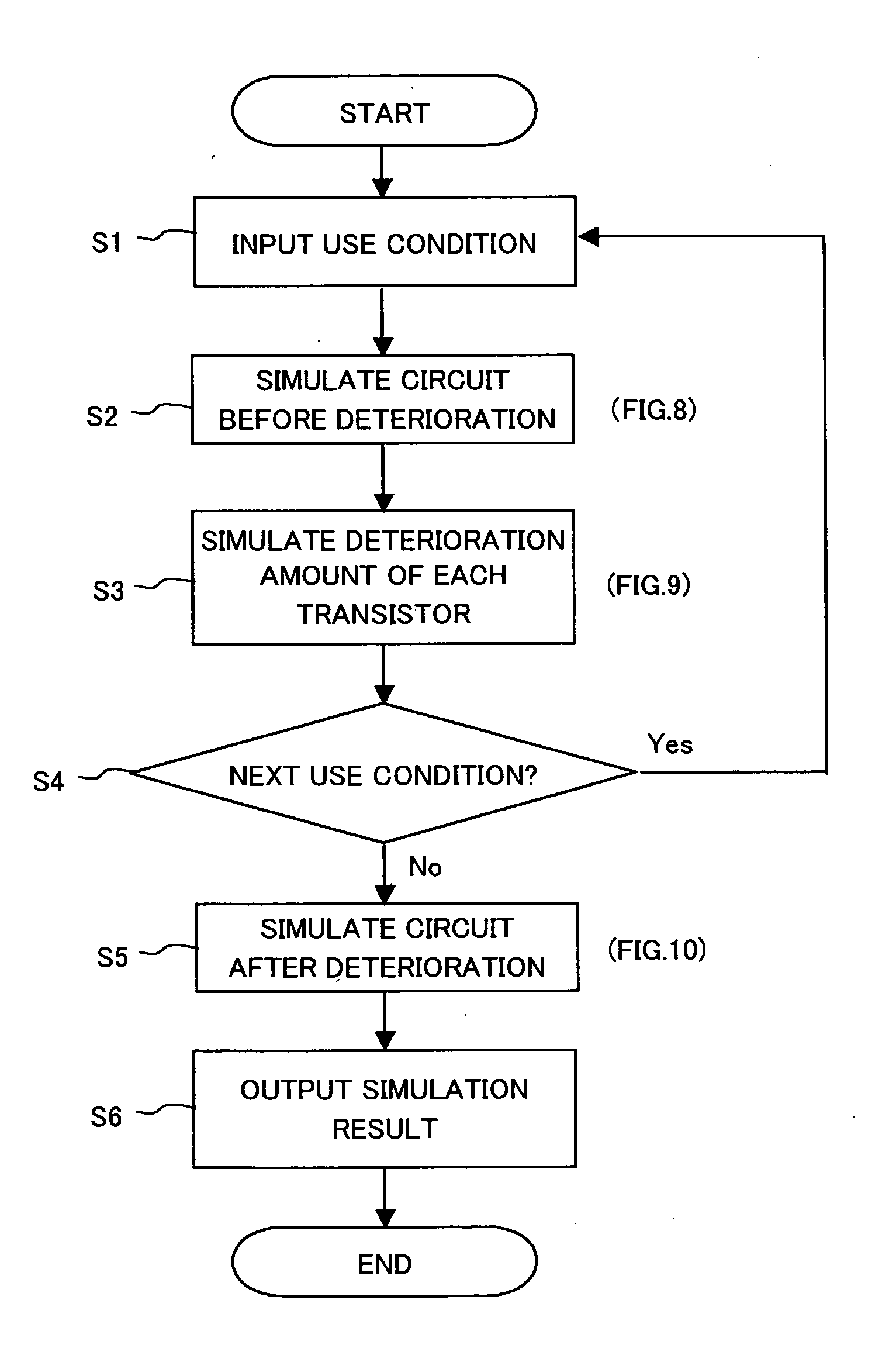
[0193] Next, as a third embodiment of the present invention, an embodiment of a semiconductor characteristics simulator for carrying out the above first embodiment will be explained.
[0194] The simulator of the third embodiment of the present invention successively performs processing of a plurality of stress conditions imposed on a transistor in a semiconductor production step and in use by a user and use conditions, simulates deterioration and recovery of characteristics of the transistor or a circuit including the transistor, and evaluates characteristics changes of the transistor or the circuit including the transistor for one circuit composed of a MIS transistor, etc.
[0195] A part or all of deterioration of transistor characteristics and a part or all of recovery of transistor characteristics, for example, deterioration and recovery of MIS transistor characteristics in a measurement step of the transistor characteristics of applying a voltage on the transistor in a semiconduct...
PUM
 Abstract
Description
Claims
Application Information
 - R&D
- Intellectual Property
- Life Sciences
- Materials
- Tech Scout
- Unparalleled Data Quality
- Higher Quality Content
- 60% Fewer Hallucinations
Browse by: Latest US Patents, China's latest patents, Technical Efficacy Thesaurus, Application Domain, Technology Topic, Popular Technical Reports.
© 2025 PatSnap. All rights reserved.Legal|Privacy policy|Modern Slavery Act Transparency Statement|Sitemap|About US| Contact US: help@patsnap.com