Manufacturing method of semiconductor device

a manufacturing method and semiconductor technology, applied in the direction of semiconductor devices, electrical appliances, transistors, etc., can solve the problems of affecting the reaction between the transition metal and silicon, and affecting the performance of the mos transistor

Inactive Publication Date: 2005-06-23
SANYO ELECTRIC CO LTD
View PDF3 Cites 5 Cited by
  • Summary
  • Abstract
  • Description
  • Claims
  • Application Information

AI Technical Summary

Benefits of technology

[0021] The invention provides a method of manufacturing a semiconductor device. The method includes forming a gate insulation film on a substrate. The substrate has a top surface portion made of silicon, and the gate insulation film is placed on the top surface portion. The method also includes forming a layer of a gate electrode material on the gate insulation film, forming a gate cover insulation film on the layer of the gate electrode material, forming a gate electrode by patterning the layer of the gate electrode material and the gate cover insulation film, injecting a low dose of a first impurity of a first conductivity type into the substrate using the gate electrode as a mask, forming a first insulation film over the substrate dosed with the first impurity, forming a second insulation film on the first insulation film, and dry-etching the second insulation film to leave only a portion of the second insulation film that is on a side wall of the gate electrode. The left portion of the second insulation film works as a spacer and is placed on a portion of the first insulation film covering the side wall of the gate electrode. The method further includes injecting a high dose of a second impurity of the first conductivity type into the substrate having the spacer, removing by a first wet etching a portion of the first insulation film that is on the gate cover insulation film of the gate electrode and another portion of the first insulation film that is on a portion of the gate insulation film that is not covered by the gate electrode, removing by a second wet etching the spacer, the portion of the gate insulation film that is not covered by the gate electrode and the gate cover insulation film of the gate electrode, forming a transition metal film over the substrate from which the spacer is removed, and inducing a chemical reaction between the transition metal layer and silicon so that a silicide layer is formed in the top surface portion of the substrate and another silicide layer is formed in a surface of the layer of the gate electrode material.

Problems solved by technology

As a manufacturing process of a semiconductor device moves to a finer design rules, there arises a problem that characteristics of a MOS transistor decline due to a short channel effect.
Another problem is resistance increase of a gate electrode and source and drain regions due to reduced dimensions of the gate electrode and the source and drain regions.
There arise following problems when the semiconductor device having the LDD structure and the silicide layers is manufactured by the method described above.
Third, the reaction between the transition metal and silicon is hampered in regions where the carbon contamination has taken place, thus the silicide layer is not formed in elliptical regions c in FIG. 13, leaving non-reacted portions there.
However, it causes a big problem with a wafer having a thin silicon substrate 21 grown on an insulator 31 as in the case of SOI (Silicon On Insulator) which has been brought into use in recent years, as shown in FIG. 14.
The transistor does not operate in some cases, because the high and low impurity concentration regions and the silicide layers are not thick enough for the transistor to operate.
There is another problem that resistances of the source and drain regions and the gate electrode vary with locations on the wafer, since an etch rate and a selection ratio of the dry-etching vary with the locations on the wafer.

Method used


Image

  • Manufacturing method of semiconductor device
  • Manufacturing method of semiconductor device
  • Manufacturing method of semiconductor device

Examples


Embodiment Construction

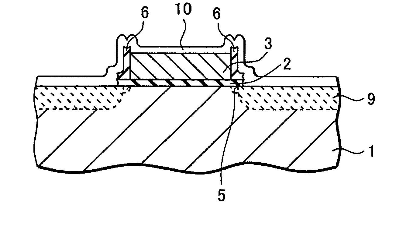
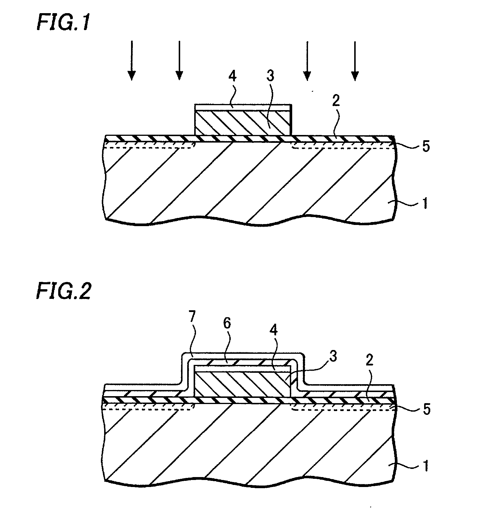
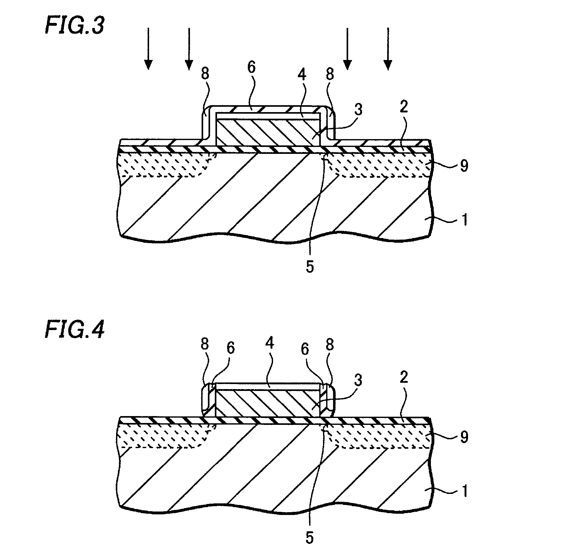
[0037] A method of manufacturing a semiconductor device according to an embodiment of this invention will be described hereafter, referring to FIGS. 1-7.

[0038] A silicon oxide film of about 5 nm in thickness is formed on a silicon substrate 1 by thermal oxidation, as shown in FIG. 1. It becomes a gate insulation film 2. And a polysilicon film of about 200 nm in thickness and an insulation film such as a silicon oxide film are formed on the gate insulation film 2. A gate electrode 3 made of the polysilicon film and the insulation film 4 stacked on it is formed by shaping the films by photolithography and etching.

[0039] After that, a low dose of impurity ions, e.g. phosphorus ions, are injected into the silicon substrate 1 using the gate electrode as a mask. In this process, about 1-5×10¹⁴ (ions / cm2) of phosphorus ions are injected into surface regions of the silicon substrate 1 about 10 nm deep from the surface of the silicon substrate 1. Subsequent heat treatment such as N2 (nitro...


PUM

PropertyMeasurementUnit
thicknessaaaaaaaaaa
thicknessesaaaaaaaaaa

Abstract

This invention offers a manufacturing method which does not cause a reduction in thickness of a silicon substrate or a carbon contamination in forming a transistor having an LDD stricture and silicide layers formed by a salicide technology. After a gate electrode is formed on the silicon substrate through a gate insulation film, an insulation film made of the same material as the gate insulation film is formed on the gate electrode. A first insulation film made of a material different from the material of the gate insulation film and the insulation film on the gate electrode and a second insulation film made of the same material as the material of the gate insulation film and the insulation film on the gate electrode are formed over the silicon substrate. Spacers made of the second insulation film are formed by dry-etching. Then the LDD structure and openings for forming the silicide layers are formed using wet-etching. As a result, the transistor having the LDD structure and the silicide layers formed by the salicide technology is manufactured without causing the reduction in thickness of the silicon substrate or the carbon contamination.

Description

CROSS-REFERENCE OF THE INVENTION [0001] This invention is based on Japanese Patent Application No. 2003-369270, the content of which is incorporated herein by reference in its entirety. BACKGROUND OF THE INVENTION [0002] 1. Field of the Invention [0003] This invention relates to a method of manufacturing a semiconductor device having an LDD (Lightly Doped Drain) structure, a silicide layer formed by a salicide technology and a spacer formed on a sidewall of a gate electrode. [0004] 2. Description of the Related Art [0005] As a manufacturing process of a semiconductor device moves to a finer design rules, there arises a problem that characteristics of a MOS transistor decline due to a short channel effect. A technology called LDD has been developed and used as a countermeasure against the problem. Another problem is resistance increase of a gate electrode and source and drain regions due to reduced dimensions of the gate electrode and the source and drain regions. A technology called...

Claims


Application Information

Patent Timeline
Patent Type & Authority Applications(United States)
IPC IPC(8): H01L21/311H01L21/336H01L29/45
CPCH01L21/31111H01L29/458H01L29/665H01L29/66772H01L29/6656H01L29/6659H01L29/66545
Inventor IIZUKA, KATSUHIKOOKADA, KAZUO
Owner SANYO ELECTRIC CO LTD
Why Eureka
Try Eureka