Method and apparatus for designing an integrated circuit using a mask-programmable fabric

a technology of integrated circuit and mask, which is applied in the direction of program control, cad circuit design, instruments, etc., can solve the problems of over-utilization of fpgas, the cost of generating a set of masks (30 or more masks are typically required) for a single design in a 90 nm process, and the inability to meet the requirements of the design, so as to facilitate the design of the integrated circuit

Active Publication Date: 2005-06-16
SYNOPSYS INC
View PDF11 Cites 3 Cited by
  • Summary
  • Abstract
  • Description
  • Claims
  • Application Information

AI Technical Summary

Benefits of technology

[0010] One embodiment of the invention provides a system that facilitates designing an integrated circuit using a mask-programmable fabric, which contains both mask-programmable logic and a mask-programmable interconnect. During operation, the system receives a description of a mask-programmable cell, wherein instances of the mask-programmable cell are repeated to form the mask-programmable fabric. The system uses this description of the mask-programmable cell to generate a derived library containing cells that can be obtained by programming the mask-programmable cell. Next, the system receives a high-level design for the integrated circuit. The system then performs a synthesis operation on the high-level design to generate a preliminary netlist for the high-level design, wherein the preliminary netlist contains references to cells in the derived library. Finally, the system converts the preliminary netlist into a netlist that contains references to the mask-programmable cell with the logic appropriately programmed.

Problems solved by technology

As semiconductor feature sizes continue to decrease, the cost of producing a set of masks used to manufacture a semiconductor chip has increased considerably.
For example, industry analysts predict that the cost of generating a set of masks (˜30 or more masks are typically required) for a single design in a 90 nm process will exceed one million dollars.
However, there are a number of problems with using FPGAs.
Although FPGAs provide a great amount of flexibility, FPGAs are relatively expensive in terms of area, power and delay.
For example, implementing a function using an FPGA can consume up to ten times the area and 500 times the power of a standard cell implementation.
Furthermore, FPGAs are typically located off-chip, so a considerable delay is typically involved in communicating with the FPGA.
However, a number of interconnection issues still remain.
In the case of SRAM-based FPGA technologies, the routing programmability needs access to active silicon, which gives rise to additional complications.

Method used


Image

  • Method and apparatus for designing an integrated circuit using a mask-programmable fabric
  • Method and apparatus for designing an integrated circuit using a mask-programmable fabric
  • Method and apparatus for designing an integrated circuit using a mask-programmable fabric

Examples


example routing

Fabric

[0067]FIG. 4 presents an exemplary mask-programmable fabric 400 in accordance with an embodiment of the invention. Mask programmable fabric 400 includes a two-dimensional array of MPF cells 401-412, which can be programmed by modifying vias between metal layer as described above.

example cell

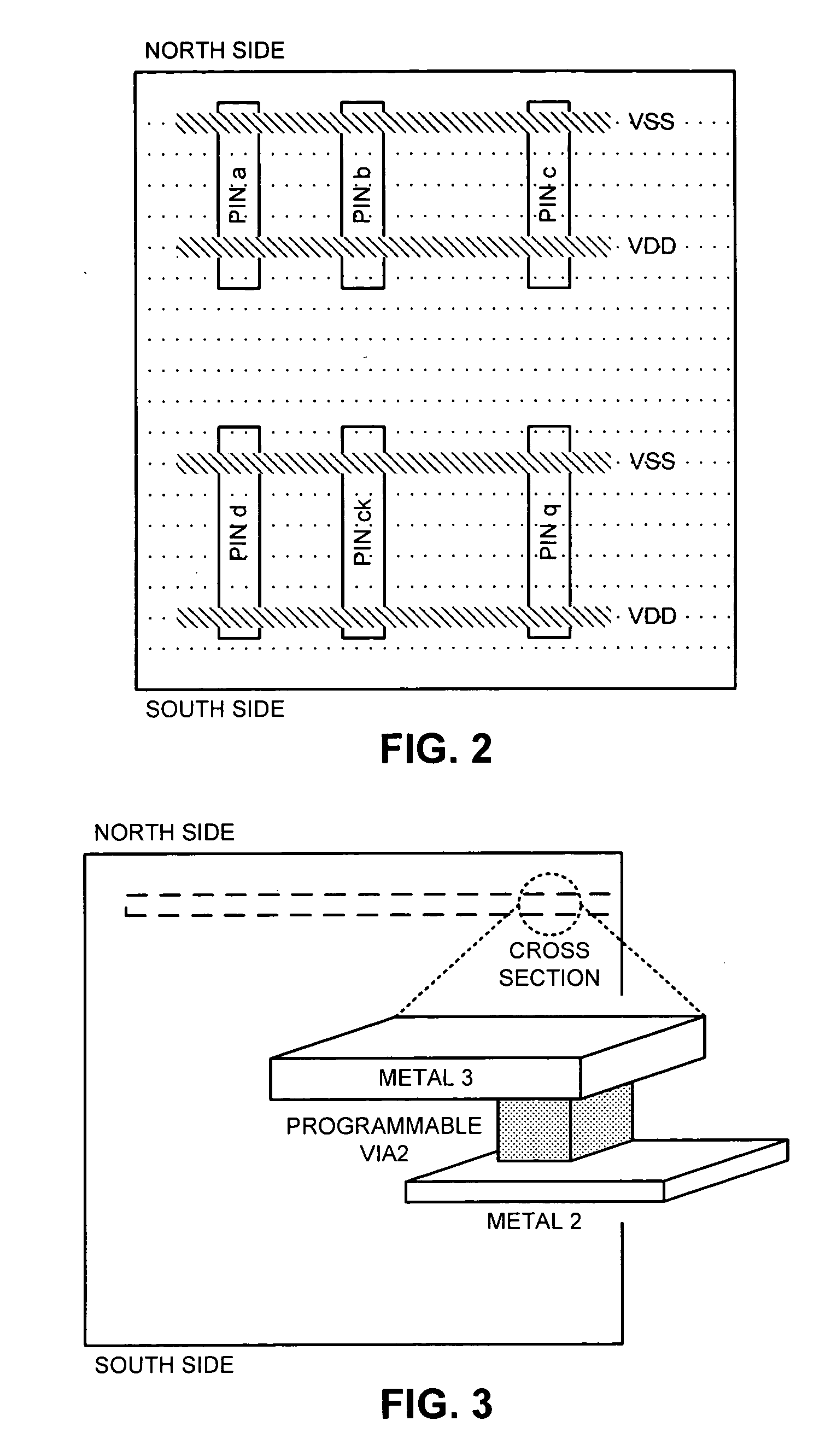
[0068]FIGS. 5A-5C illustrate the structure of a simple MPF cell. This exemplary cell is architected so that all internal connections are on metal 1, and pins appear as vertical strips on metal 2 as shown in FIG. 5A. The power and ground pins appear on the north and south edges of the cell on metal 1 and are not shown. In addition, we route power and ground on two horizontal metal 3 segments each, that intersect the vertical spans of the pins. This supports logic programming efficiently because each pin can be easily tied to power or ground by means of a via from metal 2 to metal 3. Moreover, note that each pin can connect to a horizontal metal 3 segment that intersects its vertical span for routing.

[0069] In this example, the metal 3 and metal 4 routing fabric is comprised of metal segments and is shown in FIG. 5B and FIG. 5C, respectively. Note that four segments on metal 3 are reserved for power and ground. Hence, they are unavailable for interconnect routing.

[0070] Metal 5 segm...


PUM


Abstract

One embodiment of the invention provides a system that facilitates designing an integrated circuit using a mask-programmable fabric, which contains both mask-programmable logic and a mask-programmable interconnect. During operation, the system receives a description of a mask-programmable cell, wherein instances of the mask-programmable cell are repeated to form the mask-programmable fabric. The system uses this description of the mask-programmable cell to generate a derived library containing cells that can be obtained by programming the mask-programmable cell. Next, the system receives a high-level design for the integrated circuit. The system then performs a synthesis operation on the high-level design to generate a preliminary netlist for the high-level design, wherein the preliminary netlist contains references to cells in the derived library. Finally, the system converts the preliminary netlist into a netlist that contains references to the mask-programmable cell with the logic appropriately programmed. The netlist is then placed and routed with the mask programmable constraints on the mask programmable fabric. The design, thus implemented on the programmable fabric, can be changed to accommodate logic revisions and bug fixes by changing only a few masks required for its fabrication.

Description

BACKGROUND [0001] 1. Field of the Invention [0002] The invention relates to the process of designing an integrated circuit. More specifically, the invention relates to a method and an apparatus for designing an integrated circuit using a mask-programmable fabric, which contains both mask-programmable logic and a mask-programmable interconnect. [0003] 2. Related Art [0004] The dramatic improvements in semiconductor integration densities in recent years have largely been achieved through corresponding improvements in process technologies involved in manufacturing the semiconductor chips. As semiconductor feature sizes continue to decrease, the cost of producing a set of masks used to manufacture a semiconductor chip has increased considerably. For example, industry analysts predict that the cost of generating a set of masks (˜30 or more masks are typically required) for a single design in a 90 nm process will exceed one million dollars. [0005] Note that mask re-spins are frequently re...

Claims


Application Information

Patent Timeline
Patent Type & Authority Applications(United States)
IPC IPC(8): G06F17/50
CPCG06F2217/64G06F17/5045G06F2115/06G06F30/30
Inventor SHENOY, NARENDRA V.KAWA, JAMILCAMPOSANO, RAUL
Owner SYNOPSYS INC
Why Eureka
Try Eureka