
Light emitting diode

a technology of light-emitting diodes and transmission windows, which is applied in the direction of solid-state devices, electric components, electric apparatuses, etc., can solve the problems of poor thermal stability, significant power reduction, and use of 650 nm transmission windows

Inactive Publication Date: 2005-06-16
FIRECOMMS
View PDF7 Cites 17 Cited by
  • Summary
  • Abstract
  • Description
  • Claims
  • Application Information

AI Technical Summary

Problems solved by technology

There are however two significant drawbacks of using the 650 nm transmission window of PMMA.
The first drawback is that the 650 nm transmission window is not the lowest attenuation window of PMMA, in fact the lowest attenuation windows for PMMA occur at the wavelengths of 510 nm (green) and 570 nm (amber) both of which have an attenuation of approximately −90 dBm / km for high quality POF.
The second drawback to using the 650 nm window is that the LEDs operating at this wavelength based on the semiconductor alloy AlGaInP are noted for their poor thermal stability whereby the output power significantly reduces with an increase in the ambient temperature.
However, these LEDs are not suitable for PMMA POF based data communication due to their exceedingly low efficiencies in the case of green GaAsP LEDs, and very poor thermal characteristics in regard to amber AlGaInP based LEDs.
Although some experiments have been made in demonstrating POF communication links using LEDs of this type [3] these devices are limited to a maximum modulation frequency of around 50 Mbps and have Lambertian far-field beam characteristics that lead to low coupling efficiencies into fibre and hence such devices limit the ultimate performance of the POF link.

Method used


Image

  • Light emitting diode
  • Light emitting diode
  • Light emitting diode

Examples


Embodiment Construction

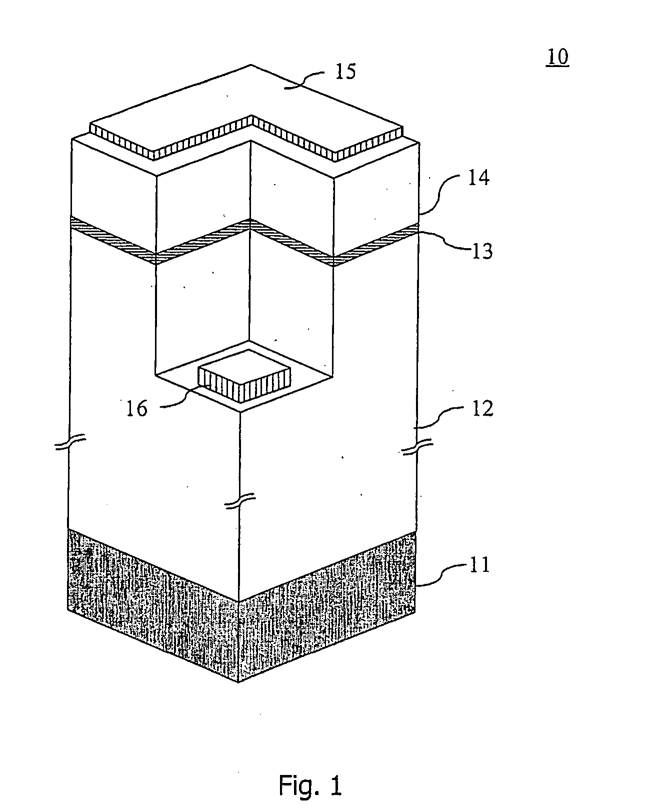
[0037]FIG. 1 is a general schematic representation of a simple embodiment of a high-speed green LED 1. The LED 1 comprises a substrate material 11, a bottom confining layer 12 of GaN heavily n-doped, an active region 13 comprising of an InxGa(1-x)N / GaN quantum well or wells whose spontaneous emission wavelength at room temperature is in the vicinity of either 510 or 570 nm, an upper GaN confinement layer 14 heavily n-doped, and a semi-transparent Ohmic contact layer 15. An Ohmic contact 16 is made to the layer 12 following the patterning and etching of the layers 12, 13 and 14.

[0038] The LED 1 may alternatively be operated embedded in a polymer material as is commonly the case in LED packaging processes, or free standing within an ambient atmosphere.

[0039] At the schematic level of FIG. 1, the LED 1 is generally similar to prior art nitride LEDs. However, it includes various advantageous features as set out below.

[0040] The free carrier life-time within the LED is minimised while...


PUM


Abstract

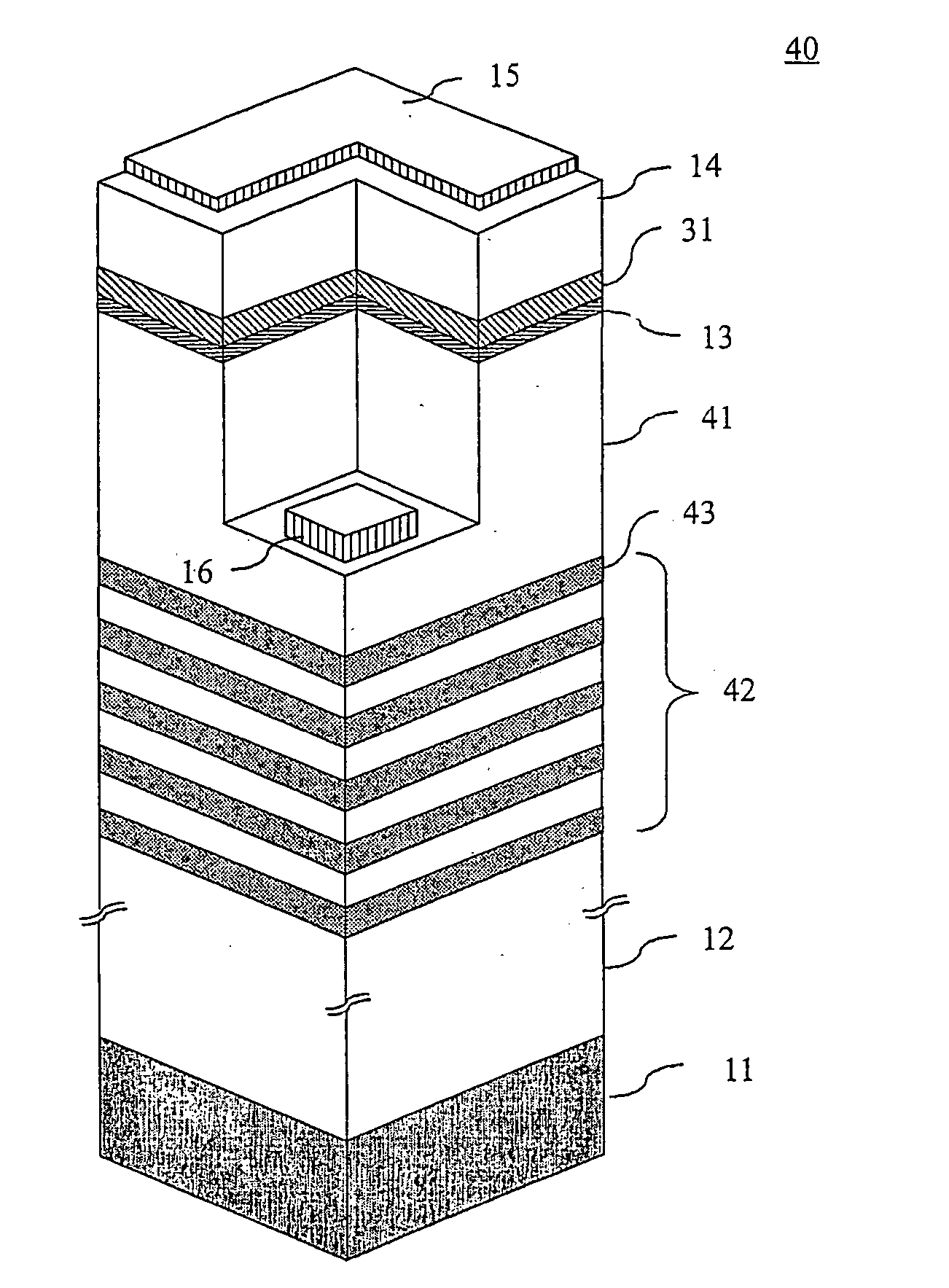
A green LED has a substrate, a GaN heavily n-doped bottom confining layer, an active region, an upper GaN confinement layer, and a semi-transparent ohmic contact layer. The active region has less than or equal to three highly compressively strained quantum wells. The widths of the quantum wells is less than 3 nm. The active region arrangement provides a short free carrier life-time and hence an increase in the modulation bandwidth of the LED.

Description

FIELD OF THE INVENTION [0001] The invention relates to light emitting diodes for optical communication. PRIOR ART DISCUSSION [0002] Plastic optical fibre (POF) has been used for many years for relatively low data rate communication applications, particularly in industrial automation applications. In this instance the use of POF enables low cost optical fibre links to be established in high electromagnetic interference (EMI) environments without resorting to more costly glass fibre links. The large core of step-index plastic optical fibre (SI-POF) and the ability to use low cost plastic-moulded connectors gives a significant cost advantage when compared to glass fibre alternatives. [0003] Due to the chemical nature of the atomic bonds of polymethylmethacrylate (PMMA), the polymer used to fabricate SI-POF, one of several attenuation windows in the POF occurs at 650 nm with an attenuation of approximately −180 dB / km. As efficient light emitting devices with an output wavelength to matc...

Claims


Application Information

Patent Timeline
Patent Type & Authority Applications(United States)
IPC IPC(8): H01L33/10H01L33/32H01L33/40
CPCH01L33/105H01L33/405H01L33/32
Inventor LAMBKIN, JOHN DOUGLASMCCORMACK, THOMAS DAVID
Owner FIRECOMMS
Learn More