Dual edge programmable delay unit

Inactive Publication Date: 2005-06-09
IBM CORP
View PDF13 Cites 3 Cited by
  • Summary
  • Abstract
  • Description
  • Claims
  • Application Information

AI Technical Summary

Benefits of technology

[0013] In accordance with this invention, a dual edge programmable delay unit is provided that includes a circuit with fast setting time, very short minimum delay time, and independent rising edge and falling edge delay time settings. The programmable delay unit of this invention can be used as real time, on-chip timing adjustment unit in a high speed system.
[0015] Preferably there are two separate controlled programmable current sources on the P side and the N side. The P side programmable source sets the charge current to the gate capacitance so that it can control the delay time at the falling edge (when the input signal VA changes from logic high to logic low). The N side programmable source sets the discharge current from the gate capacitance so that it can control the delay time at the rising edge (when the input signal VA changes from logic low to logic high). Therefore the two delay times can be adjusted independently. Since the dual edge delay times can be programmable separately, the delay unit can set different delay times for the rising edge and the falling edge, which is a feature that is especially useful in adjusting the timing of integrated circuits.
[0016] Preferably, the programmable current source consists of a pair of switching current mirrors or switching current sources that can be turned ON or turn OFF very fast on the order of picoseconds (ps). There is a code protection circuit in the delay unit, which restricts the P side current source to changing the current setting code only during the time that the input signal VA at logic high. The code protection circuit in the delay unit also restricts the N side current source to changing the current setting code only when the input signal VA is at logic low. Thus all delay times are predictable, because no delay time between two settings would occur. Due to the improved performance of the dual edge programmable delay unit, it can be used for real time and on-chip timing adjustment in integrated circuits to reach glitch free status.

Problems solved by technology

Thus the delay line of Hui '039 cannot be used in a high-speed circuit.
The rising edge and the falling edge have the same delay time, so it cannot be used as an on-chip timing adjusting unit.
The minimum delay line is long, 10 ns, so it cannot work in high speed circuits.
The rising edge and the falling edge cannot have separate delay settings, so it cannot be used as a on-chip timing adjustment unit.
The delay line operation of Hui '038 is “reset signal” based and there is no program code protection function, so it cannot be used in a real time and on-chip operation.
The delay circuit of the Phillips patent has no capability to set different delay times for rising edge and falling edge independently.
The delay circuit of the Hilton patent has no capability to set different delay times of the rising edge and the falling edge separately.
The problem with the kind of delay unit illustrated by FIG. 1 is that the rising edge delay time and the falling edge delay time are not set separately.
The result is that delay time differences are accumulated when more than one of the delay elements in series is selected.
Thus the problem is that pulse width distortion occurs in the input pulse and the output pulse from the type of circuit shown in FIG. 1.

Method used


Image

  • Dual edge programmable delay unit
  • Dual edge programmable delay unit
  • Dual edge programmable delay unit

Examples


Embodiment Construction

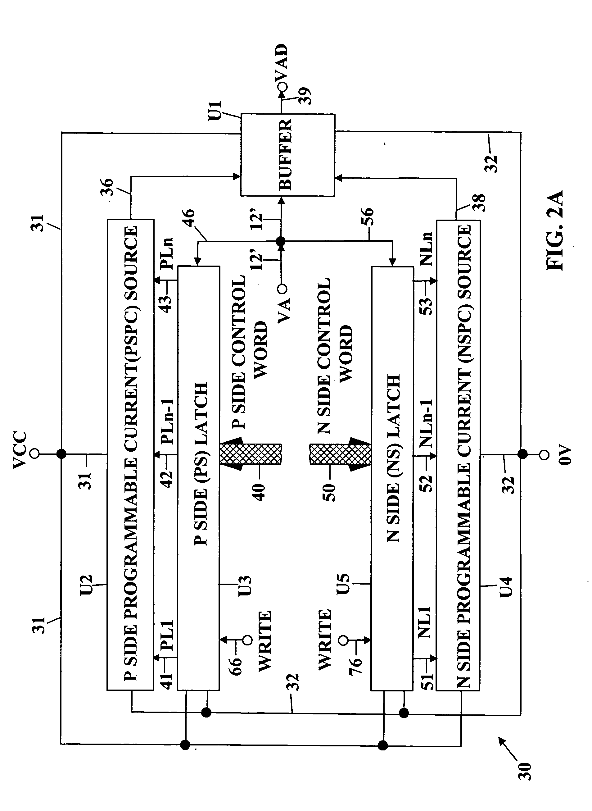
[0033]FIG. 2A is a schematic block diagram of a programmable delay unit 30 in accordance with this invention, which can independently adjust both the rising edge delay time and the falling edge delay time of an output signal VAD which is produced in response to an input signal VA.

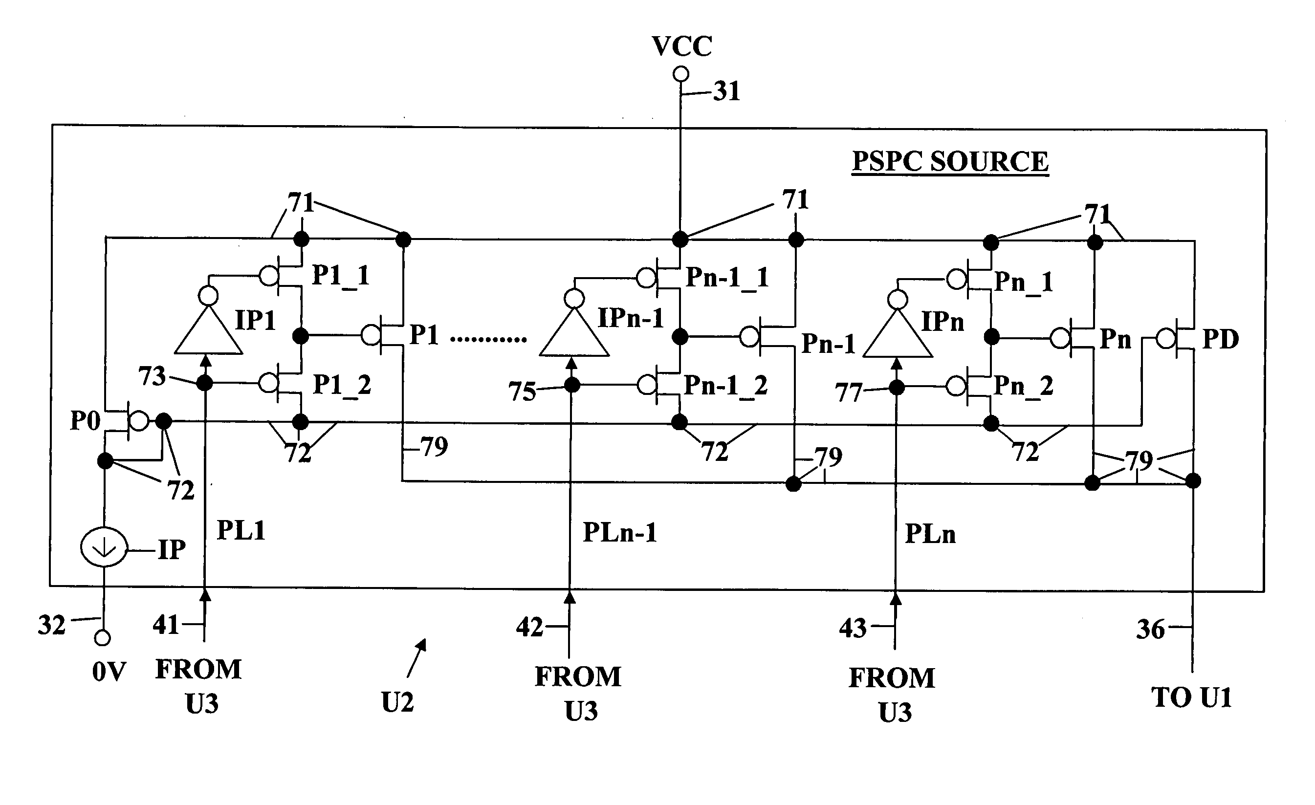
[0034] The programmable delay unit 30 shown in FIG. 2A consists of five sub-circuits. A first one of those circuits is a buffer circuit U1, which receives the input signal VA and produces the output signal VAD. The programmable delay unit 30 also includes a P side Programmable Current (PSPC) source U2, a P Side (PS) Latch U3, an N side Programmable Current (NSPC) source U4, and an N Side (NS).

[0035] The latch U3 provides digital signals to the PSPC source U2 to control the adjustment of the falling edge delay time of the output signal VAD relative to the falling edge time of the input signal VA in response to a digital input from P Side Control Word input bus 40 under control of a computer control system ...


PUM


Abstract

A method and device program a dual edge programmable delay unit, that responds to an input signal with a rise time and a fall time, includes a buffer which receives the input signal and provides an output signal with programmed variable delays between the rise and fall times of the output signal. Programmable control sources (PCS) provide separate control inputs to a buffer. The FTPCS charges a capacitor in the buffer when the input signal changes from high to low to adjust time delay before the fall of the buffer output signal. The RTPCS discharges the capacitor in the buffer when the input signal changes from low to high to adjust time delay before the rise of the buffer output signal.

Description

BACKGROUND OF THE INVENTION [0001] 1. Field of the Invention [0002] The present invention relates to programmable delay units and more particularly to providing a dual edge programmable delay unit. [0003] 2. Description of Related Art [0004] U.S. Pat. No. 5,933,039 of Hui et al (Hui '039) for “Programmable Delay Line” is related to a voltage comparator-RS register based delay line. The signal chain is long, with a minimum delay as long as 5 nanoseconds (ns). Thus the delay line of Hui '039 cannot be used in a high-speed circuit. The rising edge and the falling edge have the same delay time, so it cannot be used as an on-chip timing adjusting unit. The current source is amplifier-resistor based, and the setting time is quite long depending on the resistance selected and the parasitic capacitance. The delay line operation of Hui '039 is “reset signal” based; and no program code protection function is provided, so it cannot be used in a real time and an on-chip operation. Therefore the...

Claims


Application Information

Patent Timeline
IPC IPC(8): G01R1/00H03K5/14H03H11/26H03K5/00H03K5/06H03K5/13H03K5/1532H03K17/693H03K19/0948H03K19/173
CPCH03K5/06H03K2005/00293H03K2005/00058H03K5/13H03K5/131
Inventor FENG, KAI D.WU, HONGFEI
Owner IBM CORP
Why Eureka
Try Eureka