
Thermal treatment of solution-processed organic electroactive layer in organic electronic device

a technology of electroactive layer and organic electroactive layer, which is applied in the direction of sustainable manufacturing/processing, final product manufacturing, natural mineral layered products, etc., can solve the problems of insufficient resolution, uneconomical use of traditional transistors, and inability to meet the requirements of use, so as to improve the life time and/or performance

Inactive Publication Date: 2005-06-02
ZHANG CHI
View PDF21 Cites 9 Cited by
  • Summary
  • Abstract
  • Description
  • Claims
  • Application Information

AI Technical Summary

Benefits of technology

[0014] The invention also relates to the use of heat treatment to improve the life time and / or performance of an organic electronic device containing at least one layer of solution-processed organic electroactive material, by heat-treating one or more of such solution processed layers.

Problems solved by technology

Transistors of organic materials are less expensive than traditional transistors and may be used in low end applications where lower switching speeds maybe acceptable and where it would be uneconomical to use traditional transistors.
Such alternate methods may be complex, slow, expensive, lack sufficient resolution and when patterned using the standard lithographic (wet development) techniques, expose the device to deleterious heat and chemical processes.
Structures which favor high conductivity and thus high efficiency and long operating life are contrary to the conditions preferred for low cross talk.
However, for use in pixellated displays, the PANI(ES) or the like buffer layer needs to have a high electrical sheet resistance, otherwise lateral conduction causes cross-talk between neighboring pixels.
The resulting inter-pixel current leakage significantly reduces the power efficiency and limits both the resolution and the clarity of the display.

Method used


Image

  • Thermal treatment of solution-processed organic electroactive layer in organic electronic device
  • Thermal treatment of solution-processed organic electroactive layer in organic electronic device
  • Thermal treatment of solution-processed organic electroactive layer in organic electronic device

Examples


example 1

[0153] PANI(ES) powder was prepared according to the following reference (Y. Cao, et al, Polymer, 30(1989) 2307). The emeraldine salt (ES) form was verified by the typical green color. HC 1 in this reference was replaced by poly(2-acrylamido-2-methyl-1-propanesulfonic acid (PAAMPSA) (Aldrich). First, 30.5 g (0.022 mole) of 15% PAAMPSA in water (Aldrich) was diluted to 2.3% by adding 170 ml water. While stirring, 2.2 g (0.022M) aniline was added into the PAAMPSA solution. Then, 2.01 g (0.0088M) of ammonium persulfate in 10 ml water was added slowly into the aniline / PAAMPSA solution under vigorous stirring. The reaction mixture was stirred for 24 hours at room temperature. To precipitate the product, PANI(ES), 1000 ml of acetone was added to the reaction mixture. Most of the acetone / water was decanted and then the PANI(ES)-PAAMPSA precipitate was filtered. The resulting gum-like product was washed several times with acetone and dried at 40° C. under dynamic vacuum for 24 hours.

[0154]...

example 2

[0155] Solution / Dispersion 200 of Table 1 above was prepared.

[0156] Four grams (4.0 g) of the PANI(ES) powder as prepared in Example 1 was mixed with 400 g of deionized water in a plastic bottle. The mixture was rotated at room temperature for 48 hours. The solution dispersion was then filtered through a lam polypropylene filter. Different concentrations of PANI(ES) in water were routinely prepared by changing the quantity of PANI(ES) mixed into the water.

[0157] This Example demonstrates that PANI(ES) can be dissolved / dispersed in water and subsequently filtered through a 1 μm filter.

example 3

[0158] Four grams (4.0 g) of polyacrylamide (PAM) (M.W. 5,000,000-6,000,000, Polysciences) was mixed with 400 ml of deionized water in a plastic bottle. The mixture was rotated at room temperature for at least 48 hours. The solution / dispersion was then filtered through a 1 μm polypropylene filter. Different concentrations of PAM were routinely prepared by changing the quantity of PAM dissolved.

[0159] This Example demonstrates that PAM can be dissolved / dispersed in water and subsequently filtered through a 1 μm filter.


PUM

PropertyMeasurementUnit
conductivityaaaaaaaaaa
temperatureaaaaaaaaaa

Abstract

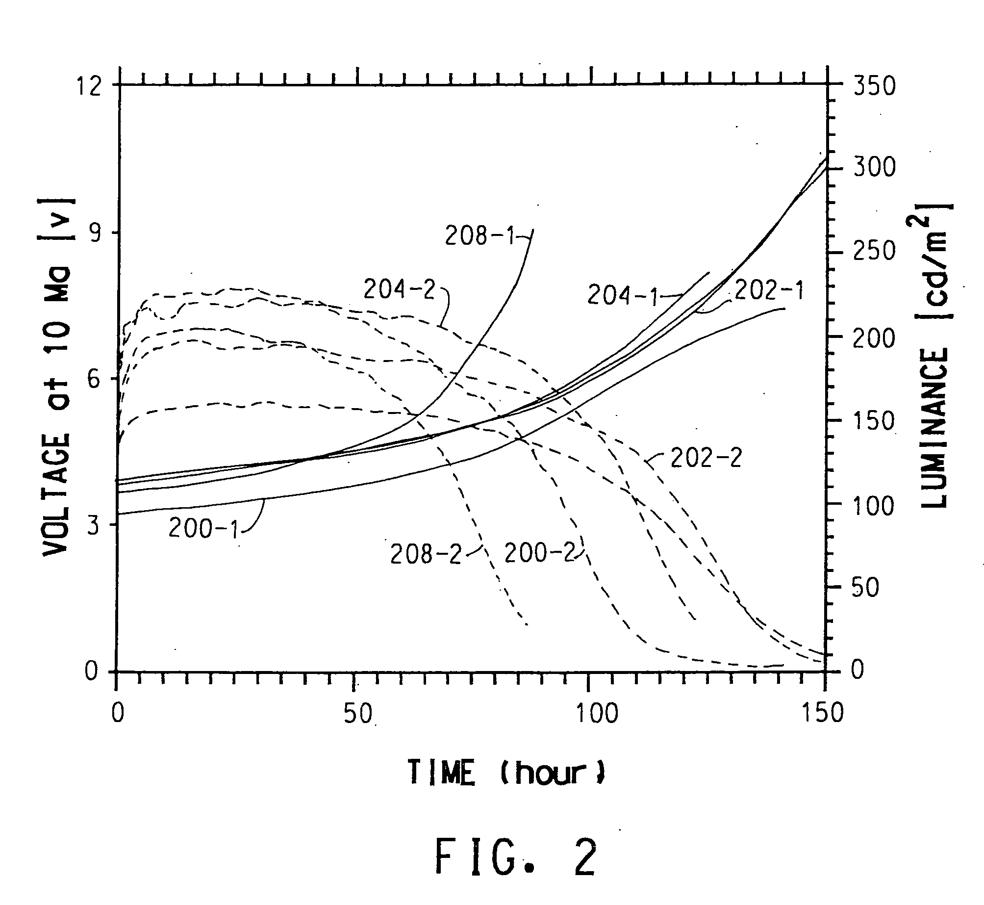
Heat treatment of conductive polymer buffer layers results in increased resistance and thus improved interpixel isolation in polymer light emitting device arrays. Heat treatment of luminescent layers results in improved lifetimes for polymer light emitting device arrays.

Description

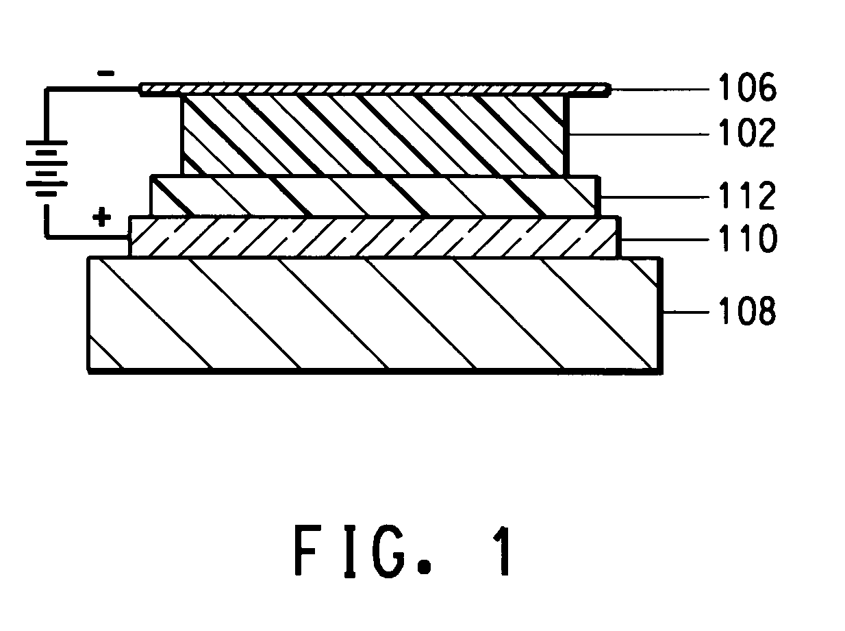
FIELD OF THE INVENTION [0001] This invention related to organic electronic devices and their fabrication. More particularly this invention relates to improvements in manufacturing such devices which can lead to improved lifetimes and / or improved performance of such devices. BACKGROUND OF THE INVENTION [0002] Organic electronic devices, such as light emitting devices, photodetecting devices and photovoltaic cells, may be formed of a thin layer of electroactive organic material sandwiched between two electrical contact layers. Electroactive organic materials are organic materials exhibiting electroluminescence, photosensitivity, charge (hole or electron) transport and / or injection, electrical conductivity, and / or exciton blocking. The material may be semiconductive. At least one of the electrical contact layers is transparent to light so that light can pass through the electrical contact layer to or from the electroactive organic material layer. Other devices with similar structures i...

Claims


Application Information

Patent Timeline
Patent Type & Authority Applications(United States)
IPC IPC(8): H01L33/00H01L33/12H01L33/26H01L33/40H10K99/00
CPCH01L51/0002H01L51/0003H01L51/0021Y02E10/549H01L51/5048H01L51/5088H01L51/5092H01L51/5012Y02P70/50H10K71/10H10K71/12H10K71/60H10K50/14H10K50/171H10K50/17H10K50/11H05B33/10
Inventor ZHANG, CHI
Owner ZHANG CHI
Learn More