Method for depositing nanolaminate thin films on sensitive surfaces
- Summary
- Abstract
- Description
- Claims
- Application Information
AI Technical Summary
Benefits of technology
Problems solved by technology
Method used
Image

Examples
example 1
The deposition of TiN from TiCl4 and NH3
[0180] A 200-mm silicon wafer coated with PVD copper was loaded into a Pulsar 2000™ ALD reactor, commercially available from ASM Microchemistry Oy of Espoo, Finland. The substrate was heated to 400° C. in a flowing nitrogen atmosphere. The pressure of the reactor was adjusted to about 5 mbar by the mass flow controller on the nitrogen line and a vacuum pump. Next, a TiNx layer was grown by ALD from sequential pulses of TiCl4 and NH3 that were separated by inert nitrogen gas.
[0181] One deposition cycle consisted of the following steps: [0182] TiCl4 pulse, for 0.05 s [0183] N2 purge for 1.0 s [0184] NH3 pulse for 0.75 s [0185] N2 purge for 1.0 s
[0186] This cycle was repeated 300 times to form about a 5-nm TiNx film. The growth rate of the TiNx film was about 0.17 Å / cycle. Then the wafer was unloaded from the reactor for analysis. Four-point probe and Energy Dispersive Spectroscopy (EDS) measurements gave a resistivity of 150 μΩcm.
[0187] Equ...
example 2
Deposition of WN from WF6 and NH3
[0189] A 200-mm silicon wafer coated with PVD copper was loaded to a Pulsar 2000 ALD reactor. The substrate was heated to 400° C. in a flowing nitrogen atmosphere. The pressure of the reactor was adjusted to about 5 mbar by the mass flow controller on the nitrogen line and a vacuum pump. Next, a WNx layer was grown by ALD from sequential pulses of WF6 and NH3 that were separated by inert nitrogen gas.
[0190] One deposition cycle consisted of the following steps: [0191] WF6 pulse for 0.25 s [0192] N2 purge for 1.0 s [0193] NH3 pulse for 0.75 s [0194] N2 purge for 1.0 s
[0195] This cycle was repeated 70 times to form about a 5-nm WNx film. The growth rate of the WNx film was about 0.6 Å / cycle. Then the wafer was unloaded from the reactor for analysis.
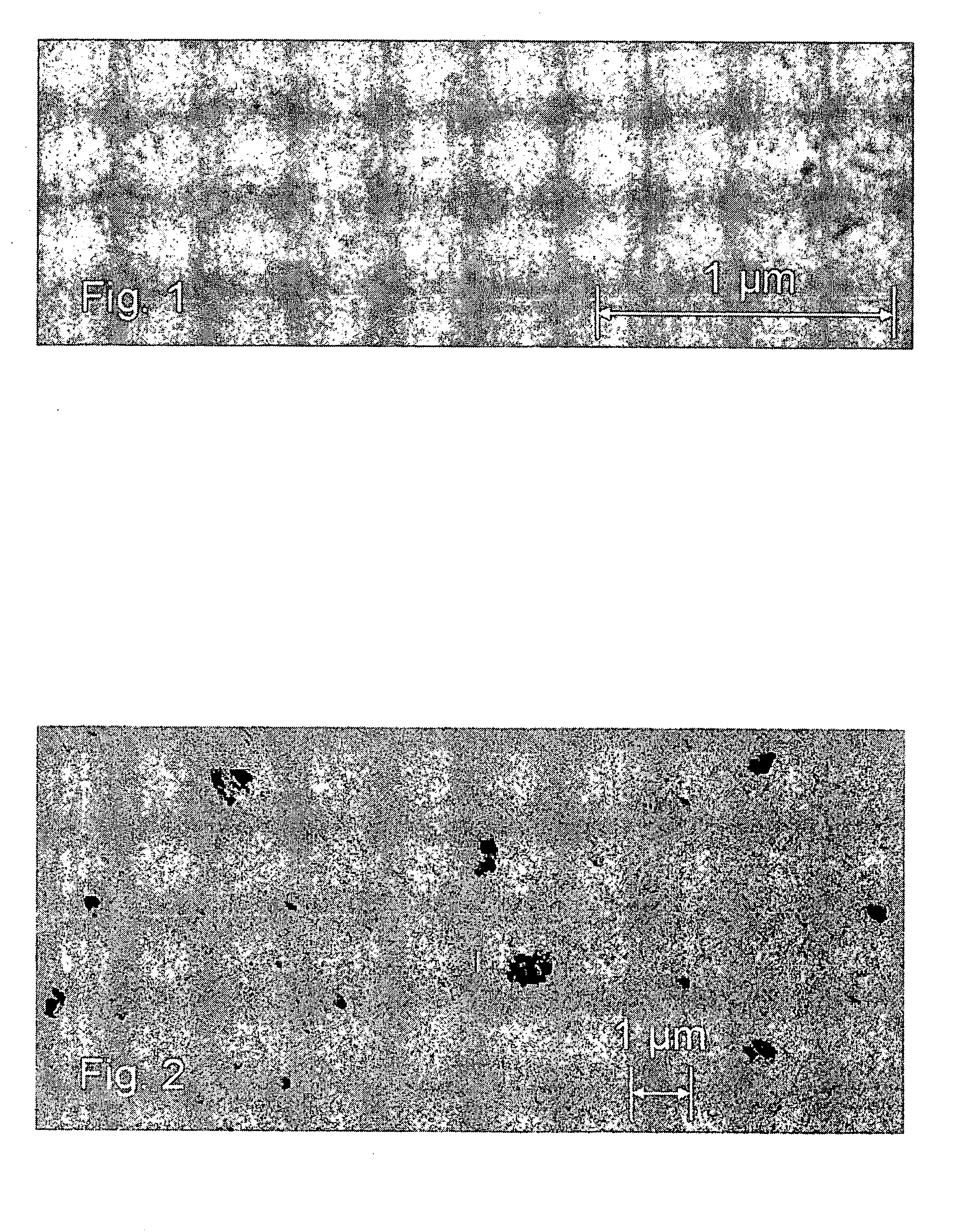
[0196] Etch damage to the copper film was visible even under an optical microscope because of the nitride process. A lot of HF was evolves from the process (R38). HF may attack the copper surface (R39). ...
example 3
Deposition of WCx with a Gettering Compound
[0197] A 200-mm silicon wafer coated with PVD copper was loaded into a Pulsar 2000™ ALD reactor. The substrate was heated to about 400° C. in a flowing nitrogen atmosphere. The pressure of the reactor was adjusted to about 5 mbar by the mass flow controller on the nitrogen line and a vacuum pump. A thin film rich in tungsten metal was grown by ALD from sequential pulses of WF6 and triethyl boron (TEB), which were separated by inert nitrogen gas.
[0198] One deposition cycle consisted of the following steps: [0199] WF6 pulse for 0.25 s [0200] N2 purge for 1.0 s [0201] TEB pulse 0.05 for s [0202] N2 purge for 1.0 s
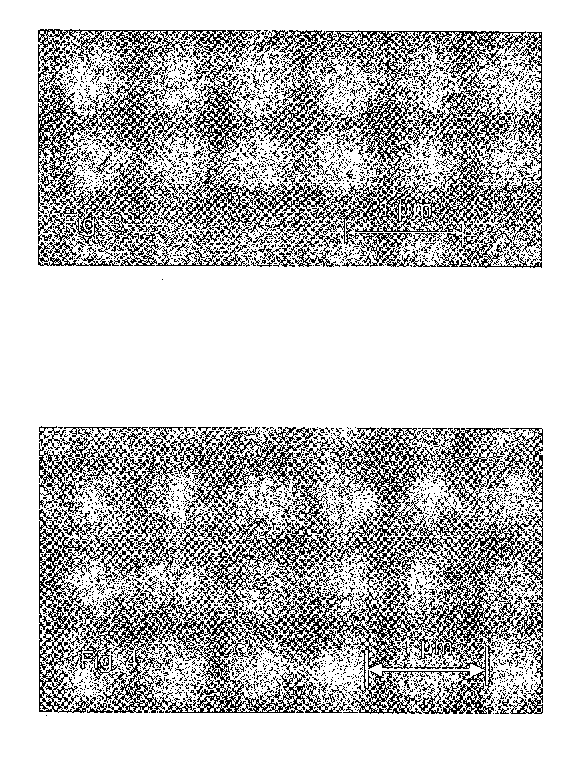
[0203] This cycle was repeated 70 times to form about a 5-nm W-rich tungsten carbide film. The growth rate of the thin film was about 0.6 Å / cycle. Then the wafer was unloaded from the reactor for analysis. No corrosion of copper was observed by Scanning Electron Microscopy (referred to as SEM hereinafter). The exact reaction mechan...
PUM
 Abstract
Description
Claims
Application Information
 - R&D
- Intellectual Property
- Life Sciences
- Materials
- Tech Scout
- Unparalleled Data Quality
- Higher Quality Content
- 60% Fewer Hallucinations
Browse by: Latest US Patents, China's latest patents, Technical Efficacy Thesaurus, Application Domain, Technology Topic, Popular Technical Reports.
© 2025 PatSnap. All rights reserved.Legal|Privacy policy|Modern Slavery Act Transparency Statement|Sitemap|About US| Contact US: help@patsnap.com