Anisotropic conductive film and method for producing the same

Inactive Publication Date: 2005-05-19
SUMITOMO ELECTRIC IND LTD
View PDF9 Cites 13 Cited by
  • Summary
  • Abstract
  • Description
  • Claims
  • Application Information

AI Technical Summary

Benefits of technology

[0030] A primary object of the present invention is to provide a new anisotropic conductive film capable of sufficiently coping with requirements of higher density mounting particularly for mounting a semiconductor package or the like because there occurs no short circuit in the plane direction of the film even if the pitch of adjacent bumps or electrodes composing a connecting portion is less than 50 μm and more preferably not more than 40 μm.
[0031] Another object of the present invention is to provide a new anisotropic conductive film particularly suitable for mounting of a contact probe or the like because it can make conductive connection more reliably by connection at a lower pressure than that in the above-mentioned case of mounting a semiconductor package, is not fused even if a large current flows, and can also cope with a high-frequency signal.

Problems solved by technology

In this case, however, the filling factor of the conductive component in the plane direction of the anisotropic conductive film is not increased.
In the range of the filling factor, however, the value of the connecting resistance in the thickness direction after thermal bonding is not sufficient, so that the number of cases where it is required that the connecting resistance should be made much lower is increasing.
In such a case, however, in the conventional anisotropic conductive film using the above-mentioned general metal powder, the insulating resistance in the plane direction of the film is also reduced, so that short circuit in the plane direction of the film easily occurs.
Since such a problem easily occurs, the conventional anisotropic conductive film cannot cope with the above-mentioned requirements unless the pitch of the adjacent bumps or electrodes composing the connecting portion is not less than 50 μm.
In the present circumstances, the conventional anisotropic conductive film cannot cope with requirements of higher density mounting in the field of electronics mounting.
Therefore, the number of times of soldering of the wirings becomes enormous.
Therefore, the manufacture of the probe card and the management thereof at the time of use are significantly difficult.
Even if the conventional anisotropic conductive film is simply used for another purpose, however, the following problems occur.
Therefore, it has been found that practical applications thereof are difficult.
However, the conventional anisotropic conductive film does not consider response to such a large current.
(ii) The contact probe is very small and is liable to be destroyed, as described above.
When the contact probe and the electrode are connected to each other at a low pressure, however, a connecting resistance in the thickness direction cannot be reduced to a sufficiently practical level, which may cause inferior connection in the conventional anisotropic conductive film.
When the filling factor of the metal powder is increased to eliminate the inferior conduction as in the item (iii), however, it is difficult to pass the high-frequency signal because the impedance of the anisotropic conductive film is increased, so that the anisotropic conductive film may be unable to be examined.
However, it is difficult for the conventional anisotropic conductive film to cope with such requirements.

Method used


Image

  • Anisotropic conductive film and method for producing the same
  • Anisotropic conductive film and method for producing the same
  • Anisotropic conductive film and method for producing the same

Examples


example 1

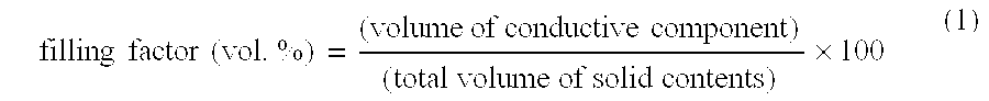
[0142] Used as a conductive component was an Ni powder, which has the form of fine Ni particles being linked in a straight-chain shape and in which the particle diameter of the Ni particles is 100 nm, the diameter D and the length L of the chain are respectively 400 nm and 5 μm, and the ratio L / D is 12.5.

[0143] The Ni powder and acrylic resin serving as a binding agent were mixed such that the filling factor of the Ni powder found in the foregoing equation (1) would be 20% by volume, and methyl ethyl ketone was added to a mixture, to prepare a paste-shaped composite material.

[0144] The composite material was then applied over a glass substrate, was dried or solidified, and was then stripped, to produce an anisotropic conductive film having a thickness of 30 μm.

example 2

[0145] An anisotropic conductive film having a thickness of 30 μm was produced in the same manner as that in the example 1 except that an Ni powder, which has the form of fine Ni particles being linked in a straight-chain shape and in which the particle diameter of the Ni particles is 400 nm, the diameter D and the length L of the chain are respectively 1 μm and 5 μm, and the ratio L / D is 5, was used as a conductive component, the Ni powder and acrylic resin serving as a binding agent were mixed such that the filling factor of the Ni powder would be 0.05% by volume, and methyl ethyl ketone was added to a mixture, to prepare a paste-shaped composite material.

example 3

[0146] An anisotropic conductive film having a thickness of 30 μm was produced in the same manner as that in the example 1 except that a metal powder having a composite structure in which a surface of an Ni powder, which has the form of fine Ni particles being linked in a straight-chain shape and in which the particle diameter of the Ni particles is 300 nm, the diameter D and the length L of the chain are respectively 600 nm and 5μ m, and the ratio L / D is 8.3, is coated with Ag having a thickness of 50 nm was used, and the metal powder and acrylic resin serving as a binding agent were mixed such that the filling factor of the metal powder would be 1% by volume, and methyl ethyl ketone was added to a mixture, to prepare a paste-shaped composite material.


PUM

PropertyMeasurementUnit
Diameteraaaaaaaaaa
Diameteraaaaaaaaaa
Percent by volumeaaaaaaaaaa

Abstract

An anisotropic conductive film, and its production method, especially suitable for mounting a semiconductor package and sufficiently satisfying the requirements of higher density mounting because short circuit does not occur in the plane direction of the film even if the pitch of electrodes is small, or suitable for mounting a contact probe because conductive connection not fused with a high current can be ensured with a lower pressure and even a high frequency signal can be dealt with. The anisotropic conductive film contains metal powder having such a shape that many fine metal particles are linked as a conductive component, wherein the length of the chain of metal powder is set not longer than the distance between adjacent electrodes being bonded conductively when a semiconductor package is mounted, and the diameter of the chain is set in the range of 1 μm-20 μm when a contact probe is mounted. At least a part of the film is formed while orienting a chain formed of a paramagnetic metal with a magnetic field.

Description

TECHNICAL FIELD [0001] The present invention relates to a new anisotropic conductive film used for electronics mounting, and a method of producing the same. BACKGROUND ART [0002] One of the methods of electronics mounting for mounting a semiconductor package on a printed circuit board, or electrically connecting respective conductor circuits on two printed circuit boards to each other and coupling or fixing both the printed circuit boards to each other is a method using a film-shaped anisotropic conductive film (see, Japanese Laid Opened Patent Publication Nos. JP-H06-102523-A2 (1994), JP-H08-115617-A2 (1996), etc.). [0003] When a semiconductor package is mounted, a semiconductor package having a plurality of bumps arranged on its mounting surface to a printed circuit board to form a connecting portion, and a printed circuit board having a plurality of electrodes arranged with the same pitch as the pitch of the bumps in its region where the semiconductor package is mounted to form a...

Claims


Application Information

Patent Timeline
IPC IPC(8): G01R1/067G01R1/073G01R3/00H01R4/04H01R43/00H05K3/32
CPCG01R1/06755G01R1/073G01R3/00Y10T428/258H01R43/007Y10T428/25H01R4/04Y10T428/31678H01B5/16
Inventor KASHIHARA, HIDEAKIYAMAMOTO, MASAMICHIYORITA, JUNTOSHIOKA, HIDEAKIOSOEGAWA, MISAKOKOYAMA, KEIJIMAJIMA, MASATOSHITANI, YOSHIE
Owner SUMITOMO ELECTRIC IND LTD
Why Eureka
Try Eureka