Semiconductor device with multi-layered wiring arrangement including reinforcing patterns, and production method for manufacturing such semiconductor device
a technology of multi-layered wiring and semiconductor devices, applied in individual semiconductor device testing, semiconductor/solid-state device testing/measurement, instruments, etc., can solve the problems of cracks, cracks, and delay in signal transmission in signal-transmission path, so as to achieve the effect of preventing cracks and peeling in the low-k insulating layer
- Summary
- Abstract
- Description
- Claims
- Application Information
AI Technical Summary
Benefits of technology
Problems solved by technology
Method used
Image
Examples
first embodiment
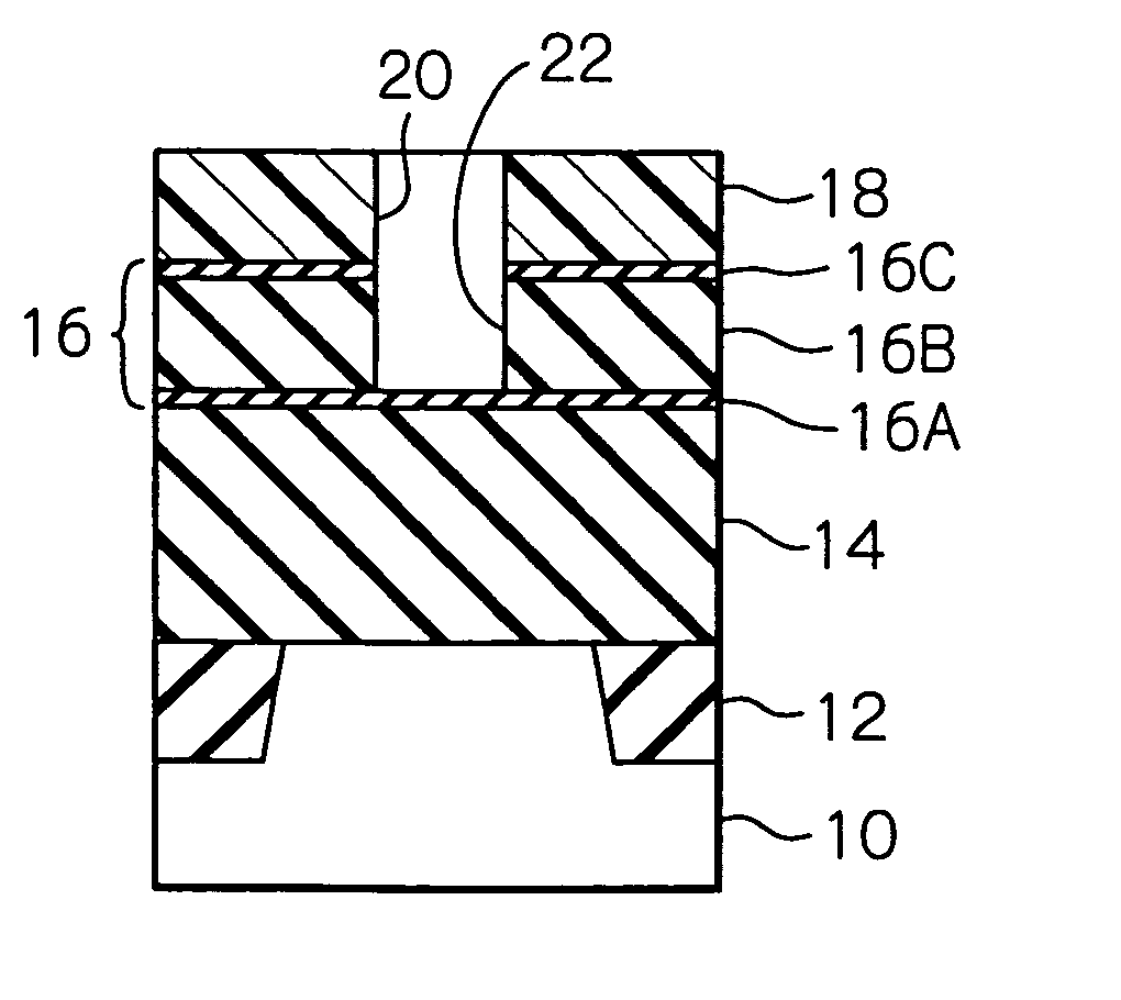
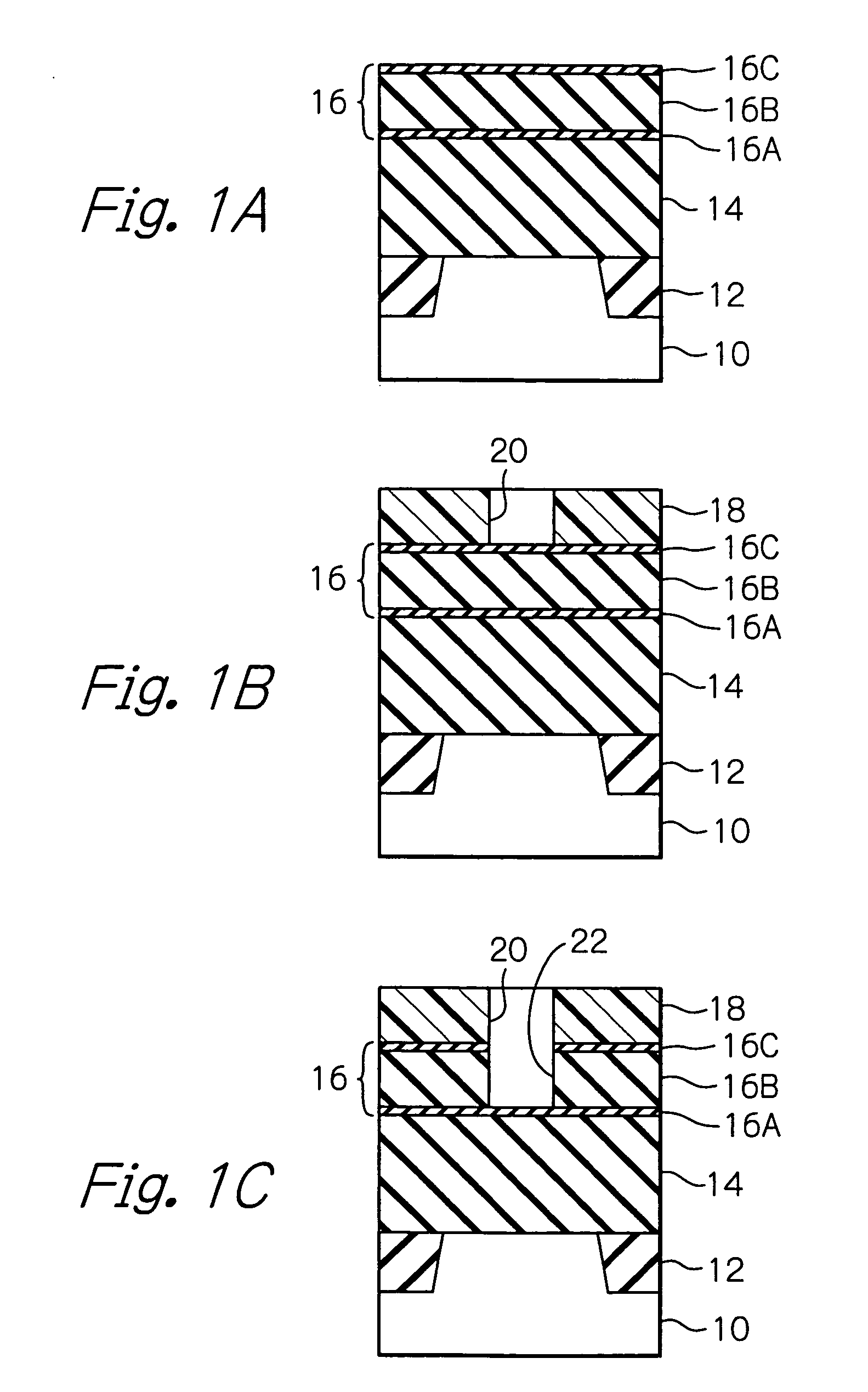
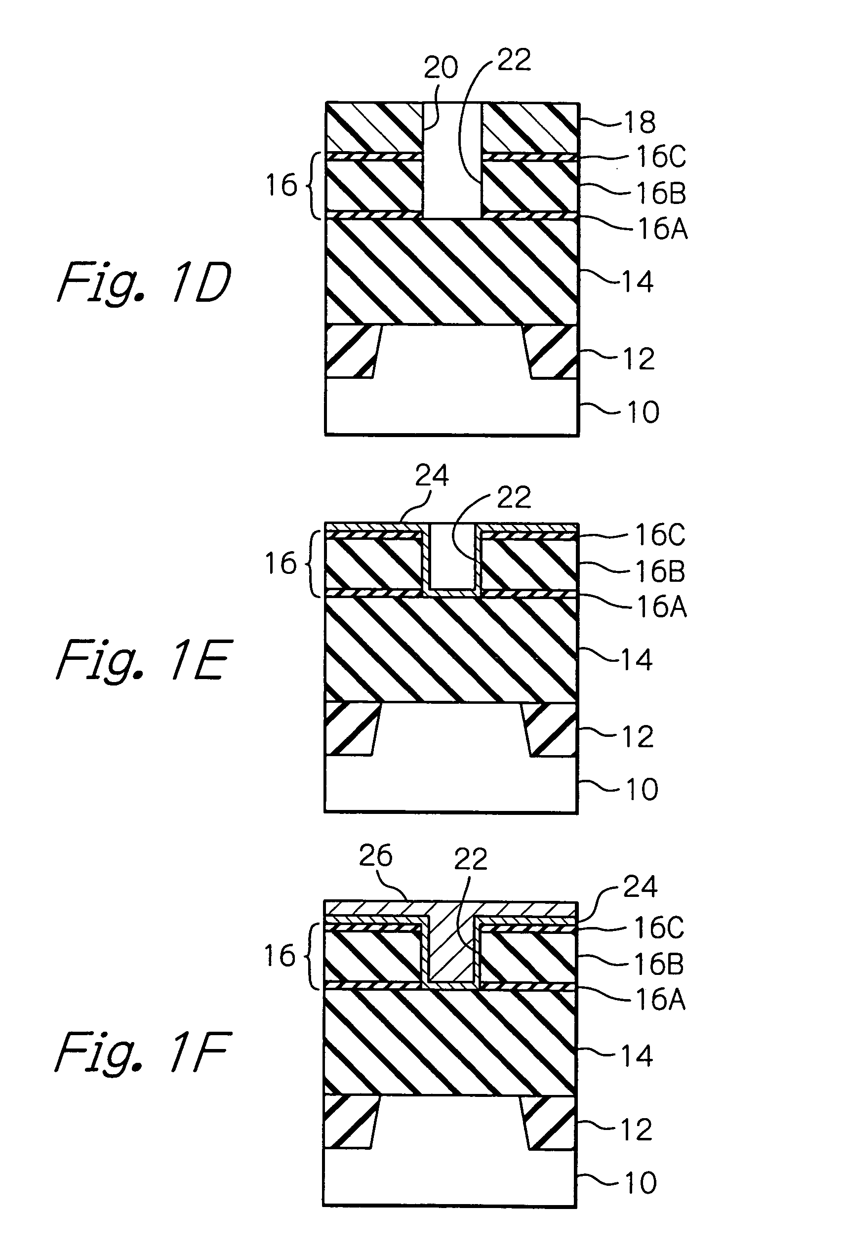
[0074] With reference to FIGS. 1A to 1N, 1P and 1Q, a production method for producing a plurality of semiconductor devices in a silicon wafer, according to the present invention, will be now explained below.
[0075] First, referring to FIG. 1A, a part of a semiconductor substrate 10, defining a semiconductor chip area on a silicon wafer, is illustrated in a vertical cross-sectional view. As shown in this drawing, an element-isolation layer 12 is formed in the semiconductor substrate 10. Note, although not visible in FIG. 1A, various elements, such as transistors, resistors, capacitors and so on, are produced in areas surrounded by the element-isolation layer 12.
[0076] After the production of the various elements is completed, a silicon dioxide layer 14 is formed as an insulating underlayer on the surface of the silicon wafer. Although not visible in FIG. 1A, contact plugs are formed in the insulating underlayer 14, and each of the contact plugs is electrically connected to a correspo...
second embodiment
[0133]FIG. 5 shows the semiconductor device according to the present invention, and this semiconductor device may be manufactured in substantially the same production method as mentioned above.
[0134] In the second embodiment, the semiconductor device includes a semiconductor substrate 114, which is derived from a silicon wafer. The semiconductor substrate 114 has an element-isolation layer 116 formed therein. Although not visible in FIG. 5, various elements, such as transistors, resistors, capacitors and so on, are produced in areas surrounded by the element-isolation layer 116.
[0135] The semiconductor device also includes a silicon dioxide layer or insulating underlayer 118 formed on the semiconductor substrate 114, and the insulating underlayer 118 has a plurality of tungsten joint plugs formed therein and connected to the semiconductor substrate. Note, in FIG. 5, only one of the joint plugs is indicated by reference 120. Of course, although not visible in FIG. 5, the insulating ...
third embodiment
[0149]FIG. 6A shows the semiconductor device according to the present invention, and this semiconductor device may be manufactured by substantially the same production method as mentioned above.
[0150] In this third embodiment, the semiconductor device includes a semiconductor substrate 146, which is derived from a silicon wafer. The semiconductor substrate 146 has an element-isolation layer 148 formed therein. Although not visible in FIG. 6A, various elements, such as transistors, resistors, capacitors and so on, are produced in areas surrounded by the element-isolation layer 148.
[0151] The semiconductor device also includes a silicon dioxide layer or insulating underlayer 150 formed on the semiconductor substrate 146, and the insulating underlayers 150 includes a plurality of tungsten joint plugs, and a plurality of tungsten contact plugs formed therein. In FIG. 6A, two of the joint plugs are indicated by references 1521 and 1522, and three of the contact plugs are indicated by re...
PUM
 Abstract
Description
Claims
Application Information
 - R&D
- Intellectual Property
- Life Sciences
- Materials
- Tech Scout
- Unparalleled Data Quality
- Higher Quality Content
- 60% Fewer Hallucinations
Browse by: Latest US Patents, China's latest patents, Technical Efficacy Thesaurus, Application Domain, Technology Topic, Popular Technical Reports.
© 2025 PatSnap. All rights reserved.Legal|Privacy policy|Modern Slavery Act Transparency Statement|Sitemap|About US| Contact US: help@patsnap.com


