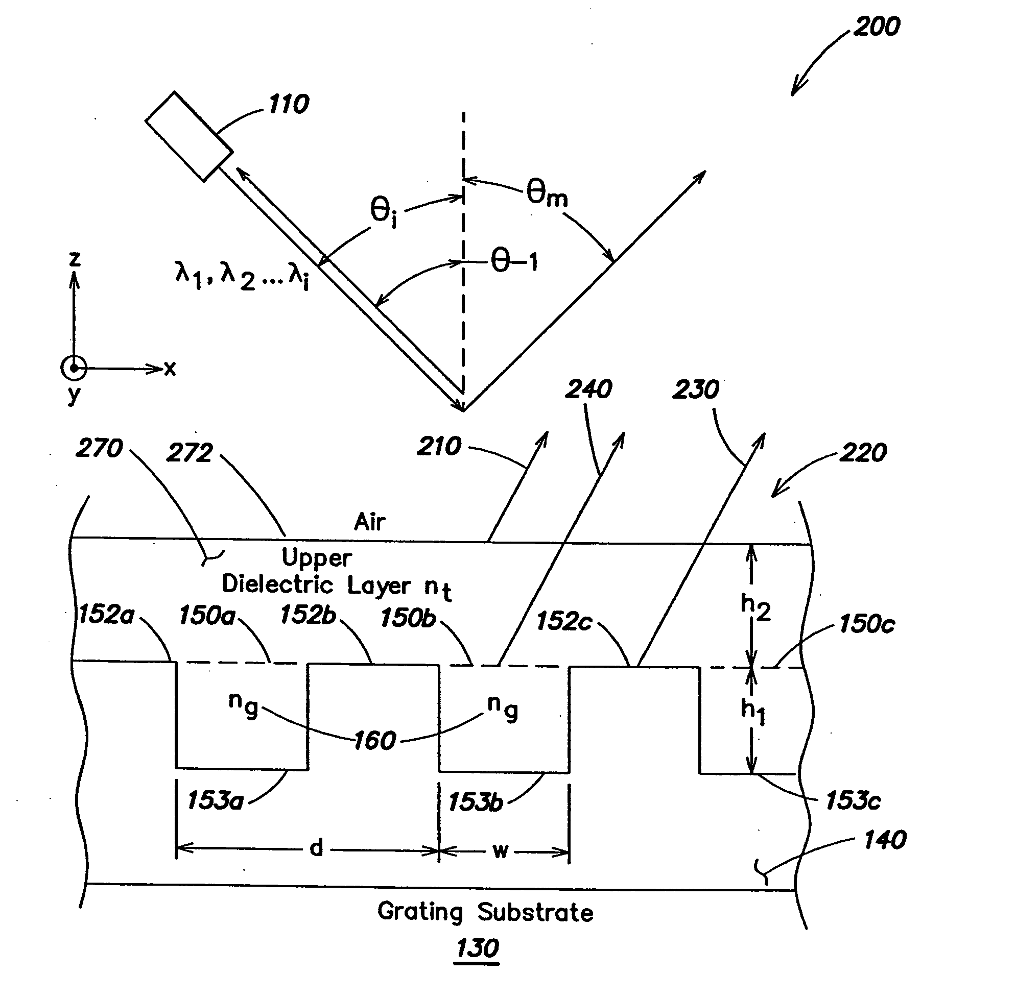
Diffraction grating having high throughput efficiency
a diffraction grating and high throughput technology, applied in the field of free space and reflective diffraction gratings, can solve the problems of low dispersion in the selected range, low efficiency of te-polarized light in this wavelength range, and single traditional gratings not being able to produce suitable amounts of each
- Summary
- Abstract
- Description
- Claims
- Application Information
AI Technical Summary
Benefits of technology
Problems solved by technology
Method used
Image
Examples
example 1
1100 Lines / mm Grating, and a Groove Depth of ¾ of the Operational Wavelength
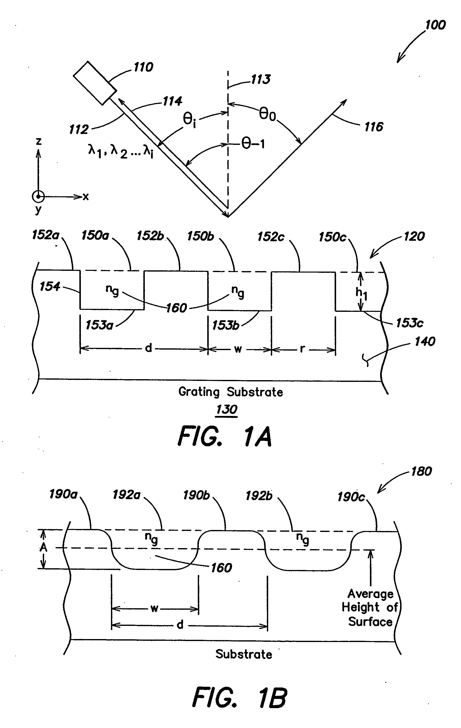
[0088] For this example, a design wavelength of 1.55 μm was chosen, which is approximately the center of the optical telecommunications C-band. A groove frequency of 1100 lines / mm was selected (i.e., a grating period of d=0.91 μm) to achieve moderately high dispersion. As determined using Equation 2, the dispersion of such a grating is 2100 μrad / nm at the Littrow angle (58.4°). An angle of incidence equal to the Littrow angle is selected, even though in practice a small angular deviation between incident and diffracted beams may be desirable, to separate the input and output beams.
[0089] The reflective material is selected to be gold, which has a refractive index nAu=0.56+9.85i. The grooves are filled with an SiO2 dielectric, which has an index of refraction ng=1.444 at the design wavelength. According to Equation 1, the groove width required for cutoff of the TM1 and TE1 modes (w≦λ / (2ng)) is w≦0.54 μm. A ...
example 2
1220 Lines / mm Grating, and a Groove Depth of ¼ of the Operational Wavelength
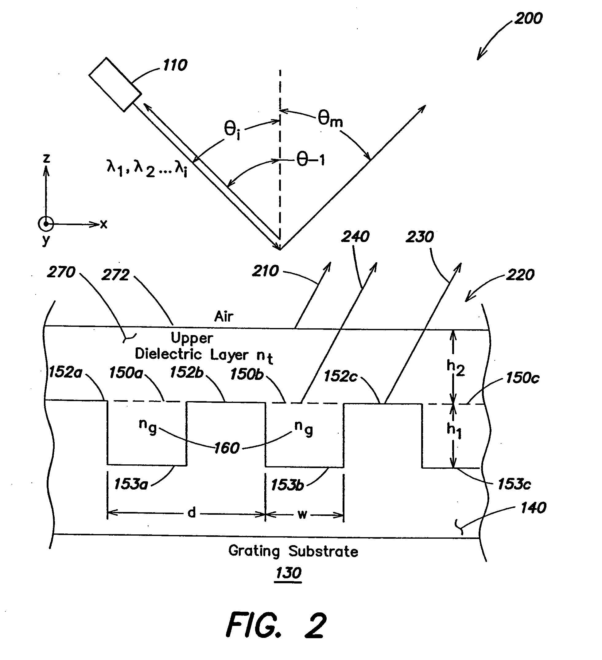
[0094] For Example 2, a design wavelength of 1.55 μm is again chosen. To obtain a higher dispersion value, the grating line frequency is selected to be 1220 lines / mm (i.e., a period of d=0.82 μm). As determined using Equation 2, the dispersion is 3700 μrad / nm at the Littrow angle (70.9°). The reflective material is again selected to be gold and groove dielectric is selected to be SiO2. The width w to achieve cutoff of the TM1 and TE1 modes is the same as above, w≦λ / (2ng), or w≦0.54 μm. However, with a smaller period and with the groove width chosen to be 80% of the width necessary to achieve cutoff of the TM-1 TE--1 modes, width w is selected to be equal to 0.52 μm. Again, this is close to a 50% duty cycle.
[0095]FIG. 6 is a graphical illustration of calculated values of TM0 TM-1 TE0 TE-1 as a function of groove depth h1 (with no overcoat layer). Because the reflective material and width w are the same as i...
PUM
 Abstract
Description
Claims
Application Information
 - R&D
- Intellectual Property
- Life Sciences
- Materials
- Tech Scout
- Unparalleled Data Quality
- Higher Quality Content
- 60% Fewer Hallucinations
Browse by: Latest US Patents, China's latest patents, Technical Efficacy Thesaurus, Application Domain, Technology Topic, Popular Technical Reports.
© 2025 PatSnap. All rights reserved.Legal|Privacy policy|Modern Slavery Act Transparency Statement|Sitemap|About US| Contact US: help@patsnap.com


