Logic circuit
a logic circuit and voltage regulation technology, applied in the field of voltage regulation technique of logic circuits, can solve the problems of increasing the likelihood of a circuit malfunction, prior art problems, and the power supply voltage cannot be reduced below approximately 1.4 v
- Summary
- Abstract
- Description
- Claims
- Application Information
AI Technical Summary
Benefits of technology
Problems solved by technology
Method used
Image
Examples
first embodiment
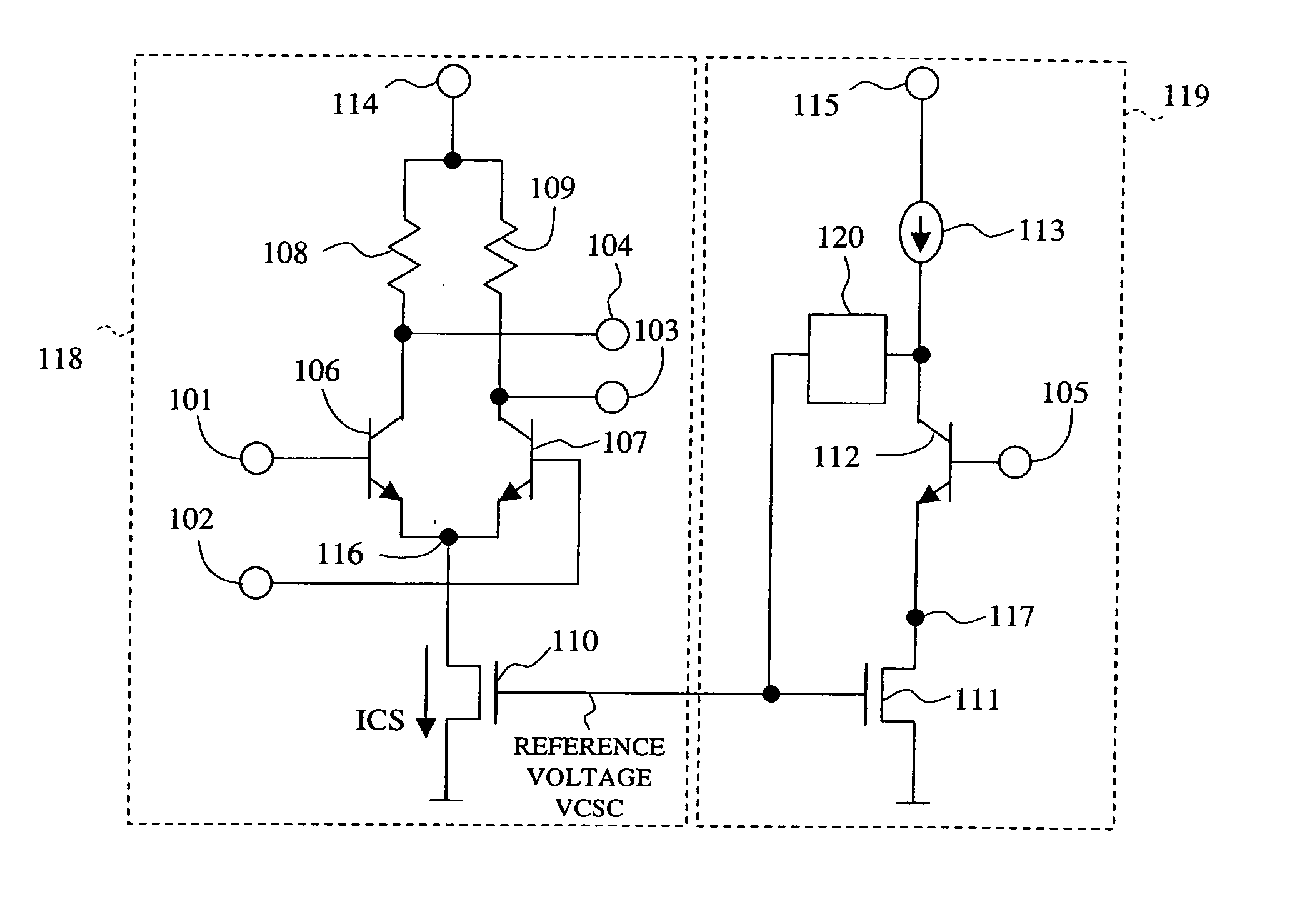
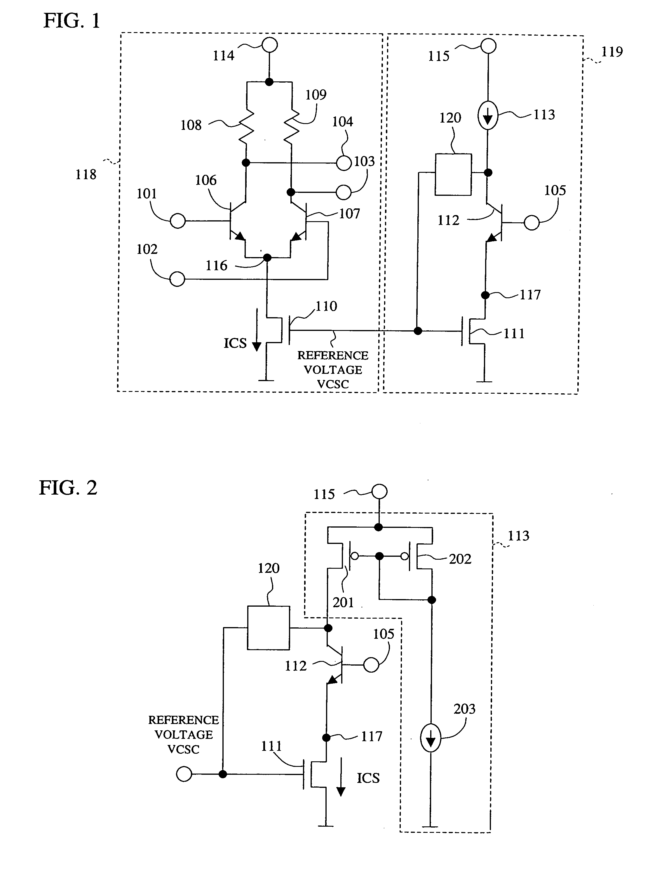
[0035] In the following, embodiments of the invention will be described with reference to the drawings. FIG. 1 shows an example of the configuration of a BiCMOS circuit according to the invention. As shown in FIG. 1, the BiCMOS logic circuit of the present embodiment includes an emitter-coupled logic circuit 118 for realizing logic functions and a reference voltage generating circuit 119 for generating a reference voltage VCSC with which to control the drain current (=current source current ICS) of a constant current-supplying n-type MOS transistor 110, which will be described later.
[0036] The emitter-coupled logic circuit 118 includes a current switch consisting of a pair of emitter-coupled bipolar transistors 106 and 107, a constant current supply n-type MOS transistor 110 connected in series with the current switch, and resistor means 108 and 109 that are connected in series with each of the bipolar transistors 106 and 107 for obtaining an output voltage.
[0037] On the other hand...
second embodiment
[0043]FIG. 2 shows an example of the configuration of a reference voltage generating circuit according to the invention. In this example, the constant current source 113 (FIG. 1) is made up of a current mirror circuit consisting of p-type MOS transistors 201 and 202, and a constant current source 203. In order to permit the p-type MOS transistors 201 and 202 to have substantially the same drain current, the voltage of the power supply 115 is set separately from the power supply 114 of the emitter-coupled logic circuit 118 so as to allow a sufficiently high voltage (1 V or higher) to be applied between the source and drain of the p-type MOS transistors 201 and 202. Further, by employing the configuration shown in FIG. 2, the power supply voltage VDD dependency of the power supply 114 regarding the current of the n-type MOS transistor 111 can be reduced. Namely, by lowering the power supply voltage VDD, the source-drain voltage VDS of the n-type MOS transistor is reduced. At the same ...
third embodiment
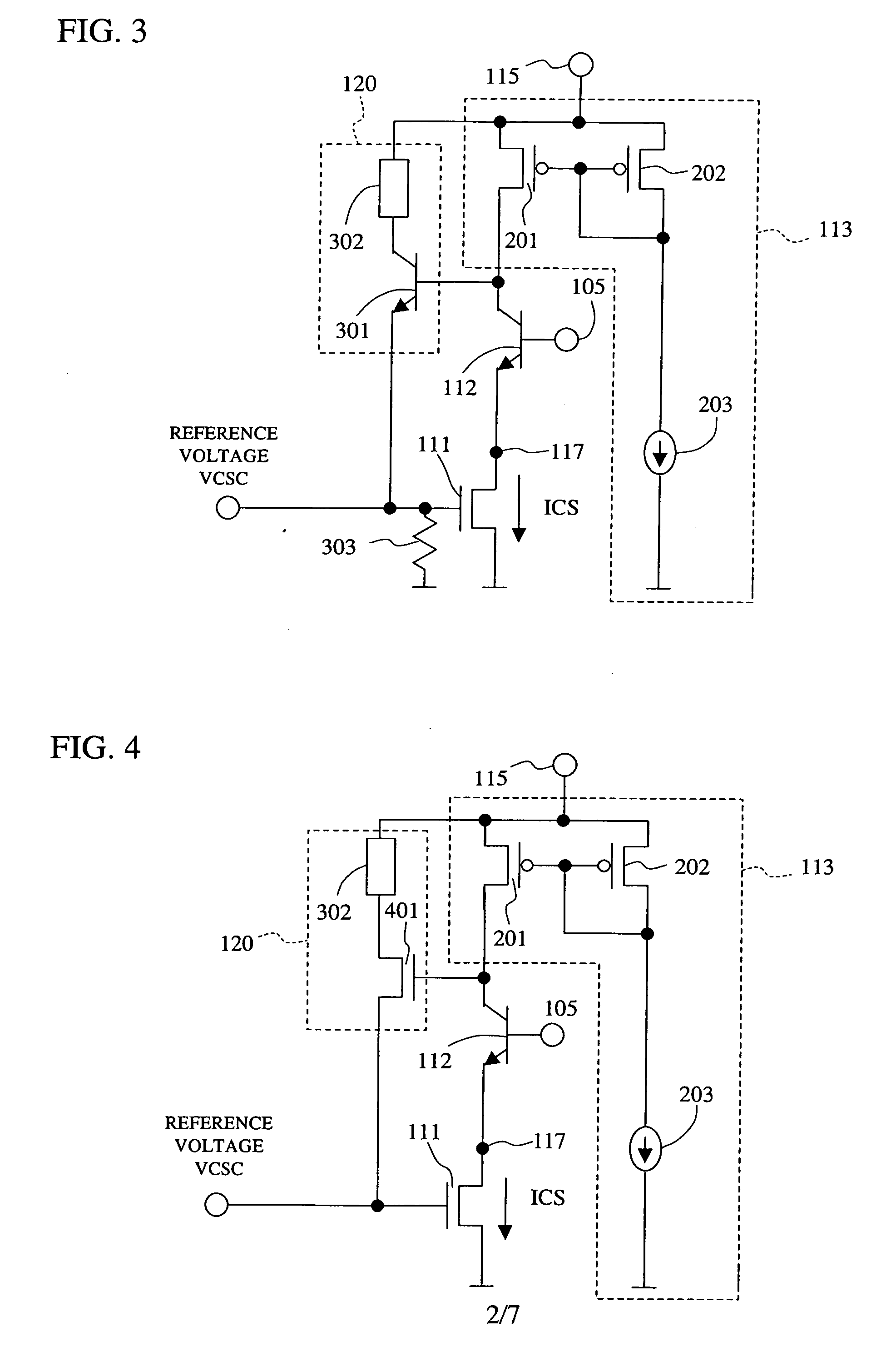
[0044]FIG. 3 shows a circuit diagram of an example of a reference voltage generating circuit adopted in a logic circuit according to the invention. In this embodiment, a first control circuit 120 comprises a bipolar transistor 301 of which the collector is connected via a resistor means 302 to a power supply 115, the base is connected to the collector of the bipolar transistor 112 for biasing the drain voltage of the n-type MOS transistor 111, and the emitter is connected to the reference voltage terminal VCSC and, via the resistor means 303, to the ground, for example.
[0045] The first control circuit 120 operates such that if the voltage at the voltage setting terminal 105 is varied, the same current flows in the n-type MOS transistor 111 as that which flows in the constant current source 203. For example, if the potential at the voltage setting terminal 105 drops, the drain voltage of the n-type MOS transistor 111 also drops, such that the drain current of the n-type MOS transisto...
PUM
 Abstract
Description
Claims
Application Information
 - R&D
- Intellectual Property
- Life Sciences
- Materials
- Tech Scout
- Unparalleled Data Quality
- Higher Quality Content
- 60% Fewer Hallucinations
Browse by: Latest US Patents, China's latest patents, Technical Efficacy Thesaurus, Application Domain, Technology Topic, Popular Technical Reports.
© 2025 PatSnap. All rights reserved.Legal|Privacy policy|Modern Slavery Act Transparency Statement|Sitemap|About US| Contact US: help@patsnap.com


