Chalcogenide phase-change non-volatile memory, memory device and method for fabricating the same

a technology of phase-change non-volatile memory and chalcogenide, which is applied in the field of memory devices, can solve the problems of further increase of device integration and device size reduction, and achieve the effect of enhancing the operation speed of chalcogenide phase-change non-volatile memory

Inactive Publication Date: 2005-03-24
MACRONIX INT CO LTD
View PDF2 Cites 191 Cited by
  • Summary
  • Abstract
  • Description
  • Claims
  • Application Information

AI Technical Summary

Benefits of technology

[0009] The object of the present invention, therefore, is to provide a chalcogenide phase-change non-volatile memory, and a memory device thereof and a method of fabricating the same. The operational speed of the chalcogenide phase-change non-volatile memory is enhanced without increasing the thickness of the chalcogenide thin film.
[0010] The present invention discloses a memory unit, which is applied to a chalcogenide phase-change non-volatile memory device. The memory unit comprises: a top electrode, a bottom electrode, and a phase-change thin film between the top electrode and the bottom electrode, wherein the phase-change thin film is a chalcogenide doped with an element therein, and the element enhances the crystallization rate of the chalcogenide. In a preferred embodiment, the element is, for example, Tin (Sn) and a mole ratio of the element within the chalcogenide is from about 0.1% to about 90%. It is preferred that the mole ratio of the element within the chalcogenide is lower than 10%.
[0011] The present invention discloses a method for fabricating a memory device, which is applied to a chalcogenide phase-change non-volatile memory. The method comprises: forming a bottom electrode; forming a phase-change thin film on the bottom electrode, wherein the phase-changed thin film is a chalcogenide doped with an element, and the element enhances the crystallization rate of the chalcogenide; and forming a top electrode on the phase-change thin film. The method of forming the phase-change thin film is performed by a sputtering process using a chalcogenide target, doped with the element therein or by a co-sputtering process using a target having the element and a chalcogenide target.
[0012] The present invention discloses a chalcogenide phase-change non-volatile memory device, comprising a word-line, a bit-line, a selective device, and a memory unit. The selective device, which is electrically coupled to the word-line and the bit-line and the memory device is electrically coupled to the selective device, wherein the memory unit comprises a top electrode, a bottom electrode and a phase-change thin film between the top electrode and the bottom electrode, and the phase-change thin film is a chalcogenide alloy doped with an element therein, the element enhancing the crystallization rate of the chalcogenide alloy. In a preferred embodiment, the element is, for example, Tin (Sn) and a mole ratio of the element within the chalcogenide alloy is from about 0.1% to about 90%. It is preferred that the mole ratio of the element within the chalcogenide alloy is lower than 10%.
[0013] In the chalcogenide phase-change non-volatile memory of the present invention, because the chalcogenide alloy within the phase-change thin film is doped with Sn which enhances the crystallization rate of the chalcogenide alloy, the operational speed of the memory is improved.

Problems solved by technology

However, increasing the film thickness prevents a further increase of the device integration and a reduction of the size of the device.

Method used


Image

  • Chalcogenide phase-change non-volatile memory, memory device and method for fabricating the same
  • Chalcogenide phase-change non-volatile memory, memory device and method for fabricating the same

Examples


Embodiment Construction

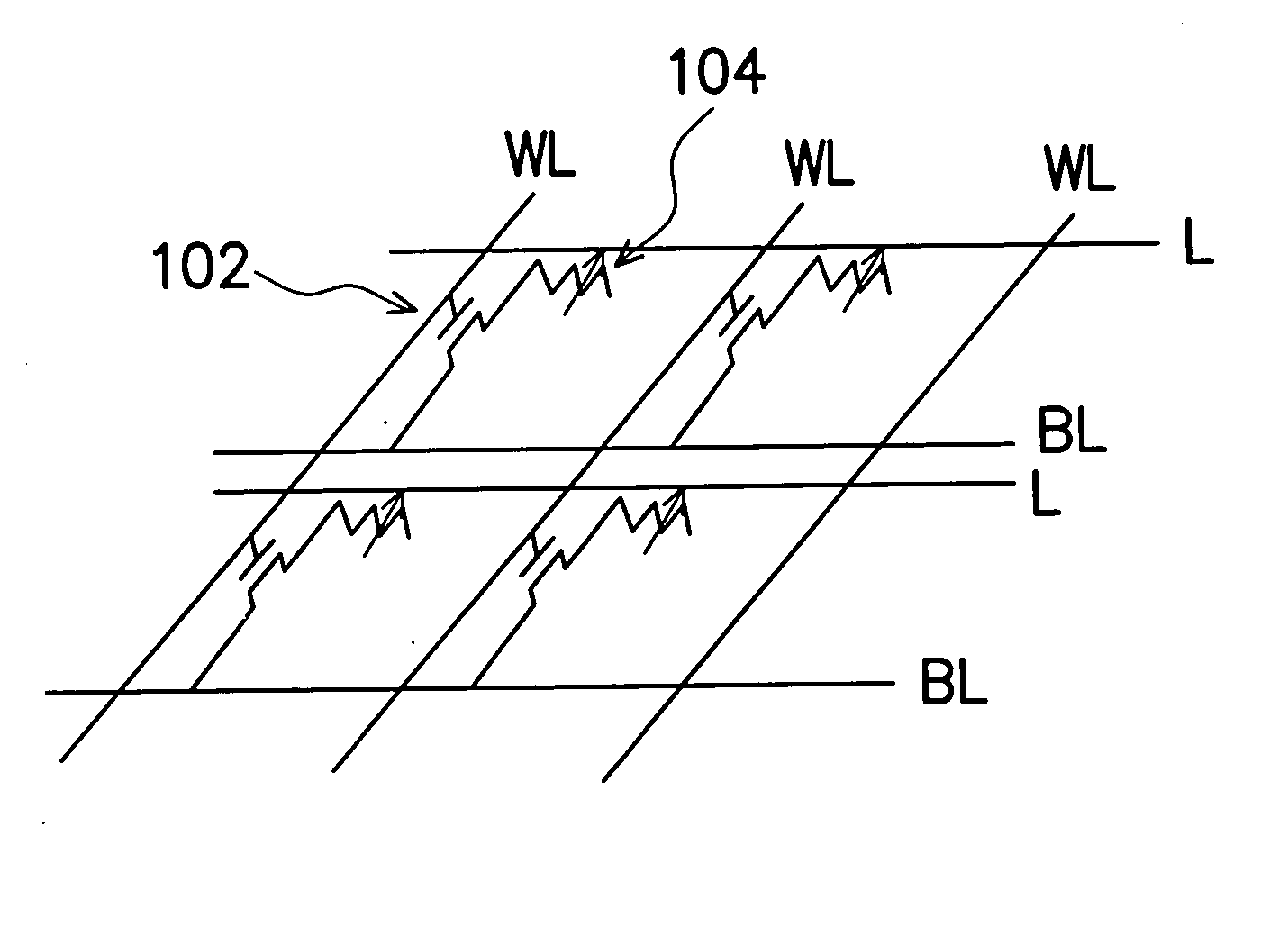
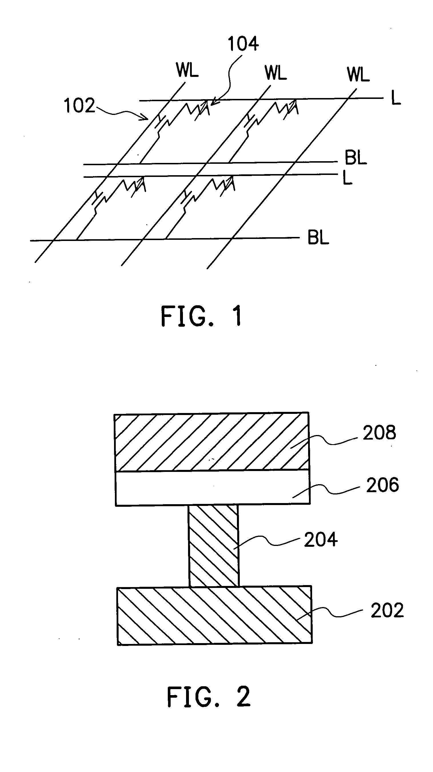
[0017] As shown in FIG. 1, it is a schematic drawing showing a preferred embodiment of a chalcogenide phase-change non-volatile memory of the present invention. Please referring to FIG. 1, the chalcogenide phase-change non-volatile memory device of the present invention is comprises of a plurality of memory cells.The chalcogenide phase-change non-volatile memory device includes word-lines, bit-lines, selective devices 102 and memory units 104. Each memory cell comprises a selective device 102 and a memory unit 104, and each selective device 102 is electrically coupled to a corresponding word-line and a corresponding bit-line. Therefore, each memory cell is controlled by a word-line and a bit-line. In a preferred embodiment, the selective device 102 is, for example, a metal-oxide-semiconductor (MOS) transistor. The word-line connects gates of MOS transistors in the same column; the bit-line connects sources of MOS transistors in the same row.

[0018] In addition, the memory unit 104 i...


PUM


Abstract

A memory device adapted to a chalcogenide phase-change memory is disclosed. The memory device comprises a top electrode, a bottom electrode, and a phase-change thin film between the top electrode and the bottom electrode. The phase-change thin film is a chalcogenide (Ge-Sb-Te) alloy doped with Tin (Sn) therein. Tin (Sn) doped in the chalcogenide (Ge-Sb-Te) alloy can enhance the crystallization rate of the phase-change thin film for improving the operation speed of the memory.

Description

CROSS-REFERENCE TO RELATED APPLICATION [0001] This application claims the priority benefits of U.S. provisional application titled “CHALCOGENIDE PHASE-CHANGE NON-VOLATILE MEMORY, MEMORY DEVICE AND METHOD FOR FABRICATING THE SAME” filed on Feb. 6. 2004. All disclosure of this application is incorporated herein by reference. This application also claims the priority benefit of Taiwan application serial no. 92125868, filed on Sep. 19, 2003.BACKGROUND OF THE INVENTION [0002] 1. Field of the Invention [0003] The present invention relates to a memory device and a method for fabricating the same, and more particularly to a chalcogenide phase-change non-volatile memory and a memory device thereof and a method of fabricating the same. [0004] 2. Description of the Related Art [0005] A non-volatile memory is a memory that can store data even if power is interrupted. A non-volatile memory which can provide multiple entry, retrieval and erasure of data, such as flash memory and nitride read only...

Claims


Application Information

Patent Timeline
IPC IPC(8): G11C16/02H01L27/24H01L45/00
CPCG11C13/0004G11C2213/79H01L45/06H01L45/1233H01L27/2436H01L45/1625H01L45/165H01L45/1658H01L45/144H10B63/30H10N70/231H10N70/826H10N70/8828H10N70/026H10N70/043H10N70/046
Inventor CHEN, YI-CHOULUNG, HSIANG-LAN
Owner MACRONIX INT CO LTD
Why Eureka
Try Eureka