Ultra low contact area end effector
a vacuum seal and end effector technology, applied in the field of end effectors, can solve the problems of backside contamination and/or damage of a wafer, difficulty in accurate wafer pick-up and transfer, and difficulty in achieving a low leakage rate vacuum seal for vacuum chuck end effectors, etc., to achieve the effect of greatly minimizing or eliminating particulate transfer
- Summary
- Abstract
- Description
- Claims
- Application Information
AI Technical Summary
Benefits of technology
Problems solved by technology
Method used
Image
Examples
first embodiment
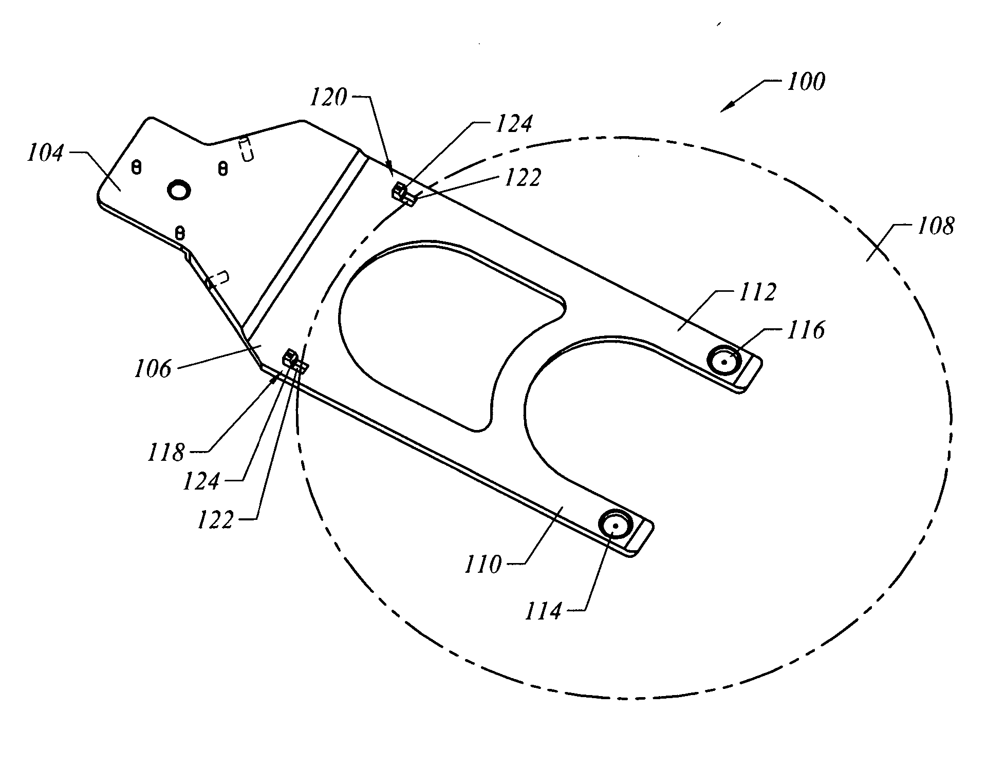
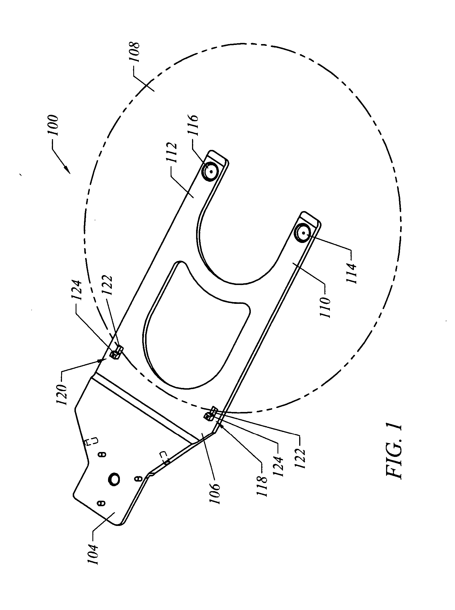
[0028] The end effector 102, in a first embodiment, includes a first end 104 adapted to secure to a wafer handling robot and a second end or platen 106 for supporting the wafer 108. The platen 106 includes a first finger 110 and a second finger 112. The first and second fingers 110, 112 are preferably spaced apart so that the first wafer support 114 and the second wafer support 116 contact different areas of the backside of the wafer 108. In this embodiment, the wafer 108 is also supported by first and second edge supports 118, 120.
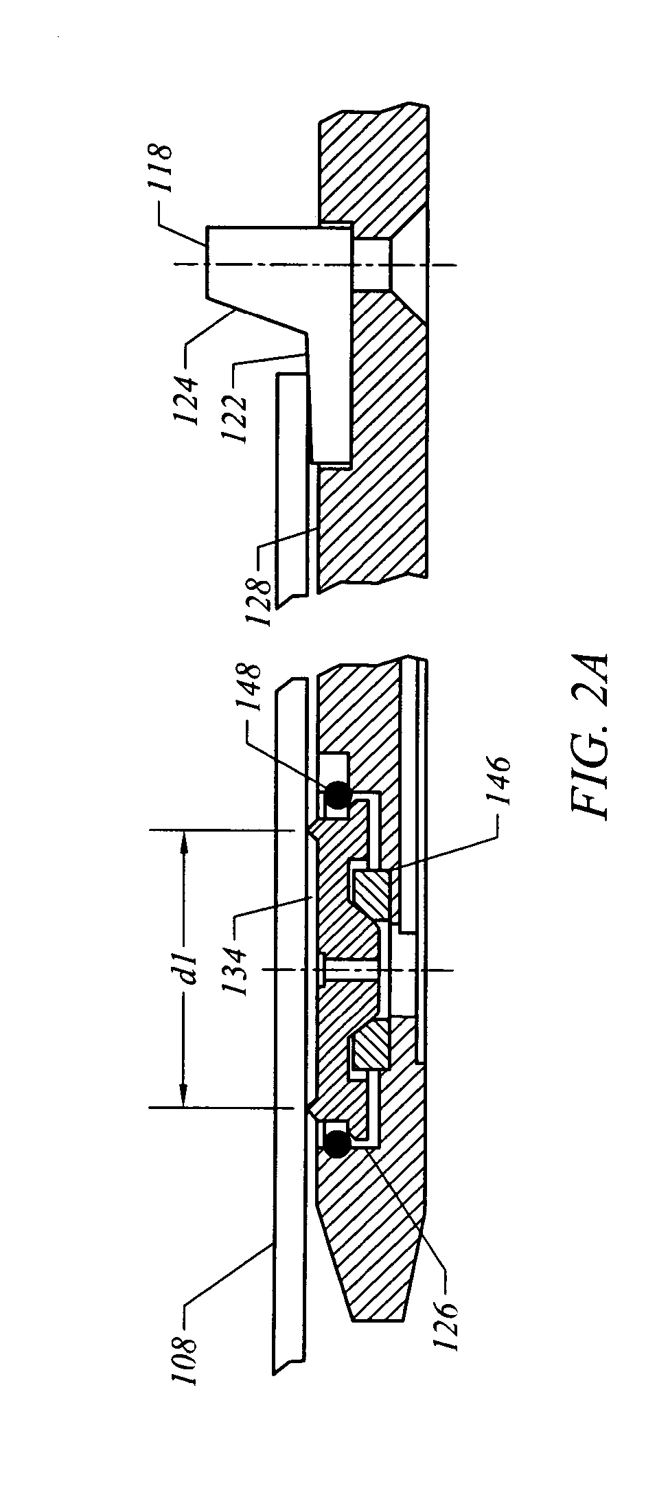
[0029]FIGS. 2A-2B illustrates that the first and second edge supports 118, 120 preferably only contact the wafer 108 along its edge or periphery. Each edge support includes a wafer support surface 122 and a backstop 124. The wafer support surface 122 is stationary and preferably comprises a low friction non-particulate generating material.
[0030] The end effector 100 includes a support retention area 126 for supporting each wafer support 114. The support ...
second embodiment
[0047] a wafer support chuck is illustrated in FIG. 7. Instead of edge supports, the wafer support chuck 214 includes a center contact ridge 232, or other support element geometries, to support the backside of the wafer. The center contact ridge 232 is the apex of the central region 234 of the wafer support chuck 214. The central region 234 comprises a conical section, as shown in FIG. 7, yet may comprise other geometries. The chuck concept could also be used in non-robotic applications, for example, on process or metrology wafer holding stations. The chucks could be arranged in a non-planar manner to produce a curved or cylindrical wafer surface.
[0048]FIG. 8 illustrates that the contact ridge 232 is preferably a rounded surface, having a radii R. Accordingly, the contact ridge 232 and the wafer's backside 130 form a contact area d. The wafer support chuck 232 also includes an outer contact area or ridge 236. The outer contact ridge 238 preferably does not contact the wafer's backsi...
PUM
 Abstract
Description
Claims
Application Information
 - R&D
- Intellectual Property
- Life Sciences
- Materials
- Tech Scout
- Unparalleled Data Quality
- Higher Quality Content
- 60% Fewer Hallucinations
Browse by: Latest US Patents, China's latest patents, Technical Efficacy Thesaurus, Application Domain, Technology Topic, Popular Technical Reports.
© 2025 PatSnap. All rights reserved.Legal|Privacy policy|Modern Slavery Act Transparency Statement|Sitemap|About US| Contact US: help@patsnap.com


