
Amorphous soft magnetic shielding and keeper for MRAM devices

a magnetic shielding layer and soft magnetic technology, applied in the direction of magnetic field-controlled resistors, semiconductor devices, semiconductor/solid-state device details, etc., can solve the problems of increasing write efficiency, reducing device power consumption, and unpractical thickness requirements of magnetic shielding layers, so as to eliminate barrier layers

Inactive Publication Date: 2005-03-03
VEECO INSTR
View PDF2 Cites 9 Cited by
  • Summary
  • Abstract
  • Description
  • Claims
  • Application Information

AI Technical Summary

Benefits of technology

[0020] One non-limiting advantage of the invention is that it uses films of amorphous soft magnetic alloys, such as CoZrTa, for magnetic shielding and keeper applications. These amorphous soft magnetic alloys have several unique advantages to allow for integration with a dual damascene Copper / SiO2 (or low-k) metallization process. Some non-limiting examples include: [0021] (i) excellent thermal stability (e.g., crystallization temperature >450° C.), making this material compatible with standard CMOS backend processing; [0022] (ii) significant permeability up to the write frequencies required in high speed memory devices (several GHz); and [0023] (iii) for the case of CoZrTa, the possibility to eliminate the barrier layer.
[0021] (i) excellent thermal stability (e.g., crystallization temperature >450° C.), making this material compatible with standard CMOS backend processing;
[0022] (ii) significant permeability up to the write frequencies required in high speed memory devices (several GHz); and
[0023] (iii) for the case of CoZrTa, the possibility to eliminate the barrier layer.
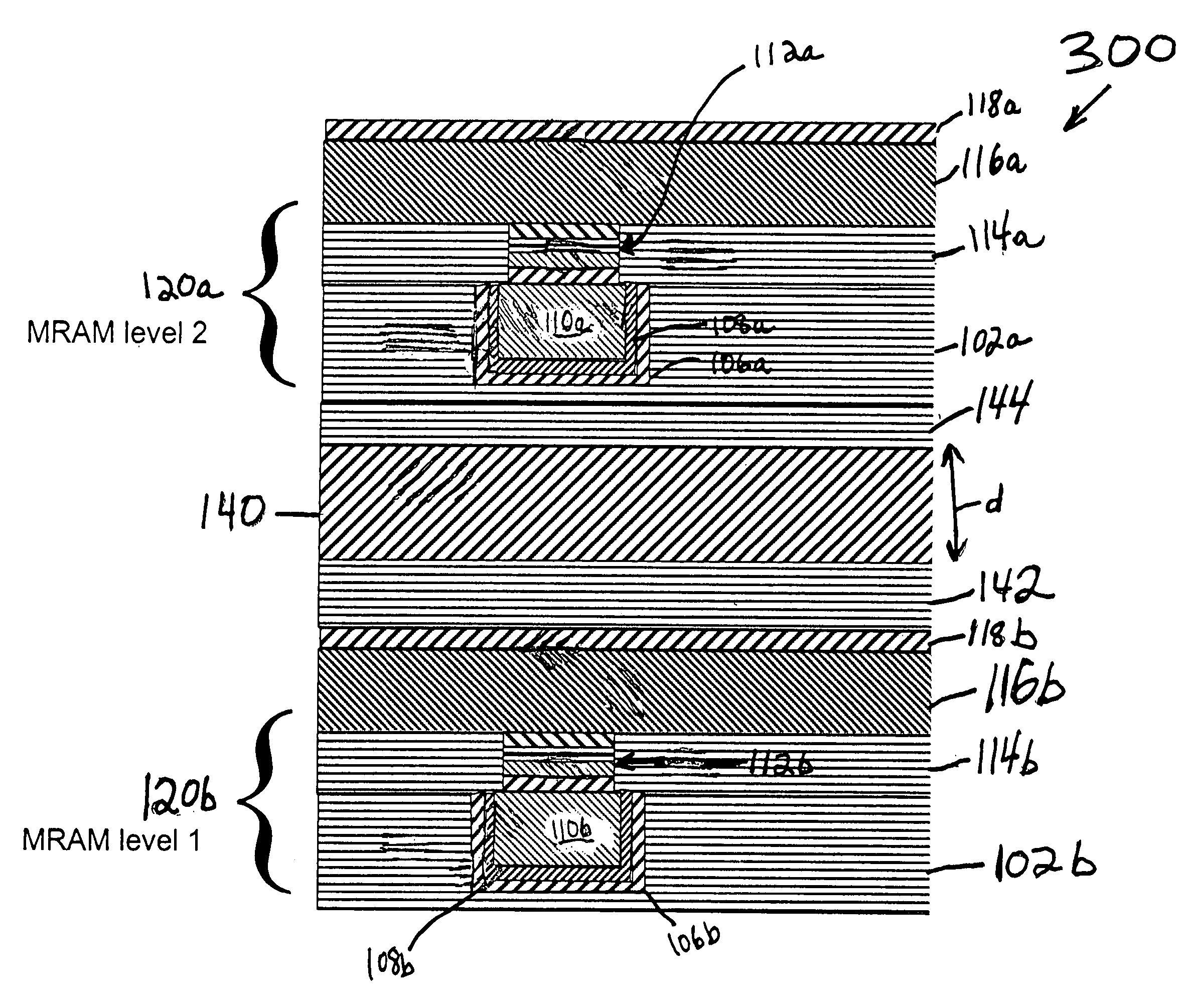
[0024] Another non-limiting advantage of the present invention is that it provides a soft magnetic shielding layer that may be introduced between subsequent layers of a multilevel metallization. This allows for the transport of large currents through metallization layers located on one side of the magnetic layer, without affecting the magnetic state of MRAM cells located on the other side of the magnetic layer.
[0025] Another non-limiting advantage of the present invention is that it provides an amorphous, soft magnetic material that can be interposed between different layers of spin-dependent tunnel junctions.

Problems solved by technology

Inserting a soft magnetic keeper around the write conductors of an MRAM device has been found to provide a desirable modification or concentration of the flux path resulting in an increase of the write efficiency, which could result in a decreased power consumption of the device.
The efficiency of shielding is proportional to the film thickness “t” multiplied by μ. Having an insufficient value of μ results in an unpractical requirement on the thickness of the magnetic shielding layer.
While above-referenced prior art teachings provide shielding and keepers for use with MRAM devices, they suffer from some drawbacks resulting from the materials that are used, which make them difficult to incorporate into a multi-layer IC metallization process.
For example, while the inventions of Tracy et al. and Durlam et al. are effective to shield MRAM devices from stray magnetic fields, they suffer from some drawbacks resulting from the types of materials used for the shielding and passivation layers.
Therefore, these materials may be unsuited for multi-layer IC fabrications in which a device undergoes one or more high temperature processes after the deposition of a shielding or passivation layer.
One drawback associated with the materials used for the keeper of Hurst et al. is that they require the use of a diffusion barrier such as TiW, TaN, or the like.
The inclusion of this additional diffusion layer undesirably complicates and increases the cost of the fabrication process.
Furthermore, it has been found that the permeability of such materials drops typically in the frequency range of tens to hundreds of MHz, due to eddy current losses and ferromagnetic resonance.
This adversely affects the operation and effectiveness of the keeper layers at frequencies relatively close to the write frequency of typical MRAM devices (e.g., several hundreds of MHz to low GHz).

Method used


Image

  • Amorphous soft magnetic shielding and keeper for MRAM devices
  • Amorphous soft magnetic shielding and keeper for MRAM devices
  • Amorphous soft magnetic shielding and keeper for MRAM devices

Examples


Embodiment Construction

[0038] The present invention will now be described in detail with reference to the drawings, which are provided as illustrative examples of the invention so as to enable those skilled in the art to practice the invention. The preferred embodiment of the soft magnetic shield and keeper and the method for forming the same are described in relation to a multi-layer MRAM fabrication procedure. However, it will be appreciated by those skilled in the art that the present invention is equally applicable to other types of fabrication procedures.

[0039] Generally, soft magnetic thin film materials can be classified in three main classes including: (1) crystalline metallic films such as Permalloy (NiFe alloys around the composition Ni80Fe20), FeXN (where X may be a metal such as Ta, Al, Ti, etc.), and the like; (2) Oxidic metallic films such as Manganese Zinc Ferrite or Nickel Zinc Ferrite; and (3) amorphous metallic films such as CoNbZr, CoTaZr or CoPdZr. While prior art MRAM fabrication pro...


PUM

PropertyMeasurementUnit
thicknessaaaaaaaaaa
temperatureaaaaaaaaaa
aspect ratioaaaaaaaaaa

Abstract

An amorphous soft magnetic thin film material for forming shielding and keeper applications in MRAM devices. The amorphous soft magnetic material may be deposited using Physical Vapor Deposition (PVD) in the presence of a magnetic field, in order to form shielding layers and keepers in a multi-layer metallization process. The soft magnetic material may be an amorphous metallic alloy, such as CoZrX, where X may be Ta, Nb, Pd and / or Rh.

Description

FIELD OF THE INVENTION [0001] The present invention generally relates to magnetic random access memory (MRAM) devices and more particularly, to an amorphous soft magnetic layer for application as a shield and keeper in MRAM devices. BACKGROUND OF THE INVENTION [0002] Magnetic Random Access Memory (MRAM) devices based on spin-dependent tunnel junctions are being explored as non-volatile solid state memory devices for embedded and stand alone applications. MRAM devices utilize magnetic material within memory cells to store data bits. The data bits are read by magnetoresistive sensing. MRAM memory cells can be programmed by magnetizing the magnetic material within the cells. The magnetic field required to switch the state of a cell (e.g., from “0” to “1”) is typically quite low, e.g., in the range of 10-25 Oersteds (Oe). [0003] In its basic concept, an MRAM memory cell typically consists of a patterned magnetic multi-layer bit region, and two conductive lines (e.g., the word and bit li...

Claims


Application Information

Patent Timeline
Patent Type & Authority Applications(United States)
IPC IPC(8): H01L21/00H01L23/552H01L27/22H10N50/01H10N50/10
CPCH01L27/222H01L43/12H01L43/08H10B61/00H10N50/01H10N50/10
Inventor KOOLS, JACQUES CONSTANT STEFANMAO, MINGSCHNEIDER, THOMASWANG, JINSONGGUTKIN, MICHAEL
Owner VEECO INSTR
Learn More