Laser thermal processing with laser diode radiation

a laser diode radiation and laser thermal processing technology, applied in the field of laser thermal processing, can solve the problems of difficult to achieve good dose uniformity over a relatively large area in a single, large amount of laser diode radiation required, and large area required for laser thermal processing,

Inactive Publication Date: 2005-03-03
VEECO INSTR
View PDF19 Cites 41 Cited by
  • Summary
  • Abstract
  • Description
  • Claims
  • Application Information

AI Technical Summary

Benefits of technology

A second aspect of the invention is a method of performing laser thermal processing (LTP) of a substrate using laser diode radiation. The method includes emitting radiation of a select wavelength from a two-dimensional array of laser diodes, receiving the emitted radiation with an LTP optical system, and irradiating the substrate with a radiation beam that forms a line image at the substrate. The radiation beam is incident on the substrate at an incident angle at or near the Brewster's angle for the substrate. The method also includes scanning the line image over at least a portion of the substrate so that each scanned portion of the substrate sees a pulse of laser radiation. This pulse takes the surface temperature of the silicon substrate to within 400° C. or less of the melting point of silicon (1410° C.) for a period between 100 μs and 20 ms.

Problems solved by technology

Because the required field size can exceed four (4) centimeters-squared (cm2) and the required dose can exceed one (1.0) Joules / cm2, a relatively large, expensive laser is required.
It is also difficult to achieve good dose uniformity over a relatively large area in a single pulse because the narrow spectral range of most lasers produces a speckled pattern due to interference effects.
However, performing laser thermal processing with a linear array of laser diode bars as described in the '681 patent is problematic.

Method used


Image

  • Laser thermal processing with laser diode radiation
  • Laser thermal processing with laser diode radiation
  • Laser thermal processing with laser diode radiation

Examples


Embodiment Construction

The apparatus of the present invention is first described, followed by its methods of operation. The power density requirements and system throughput capabilities are then set forth.

Apparatus

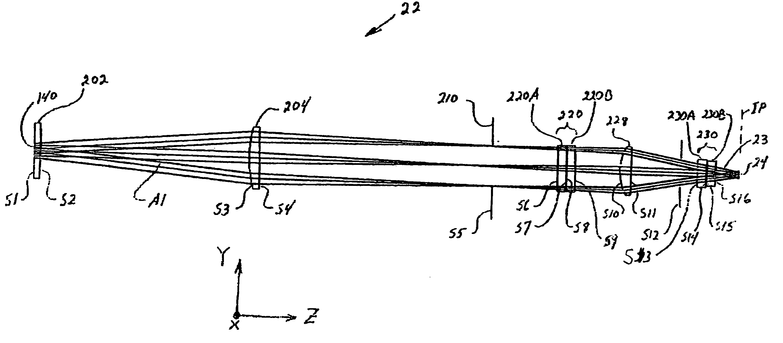
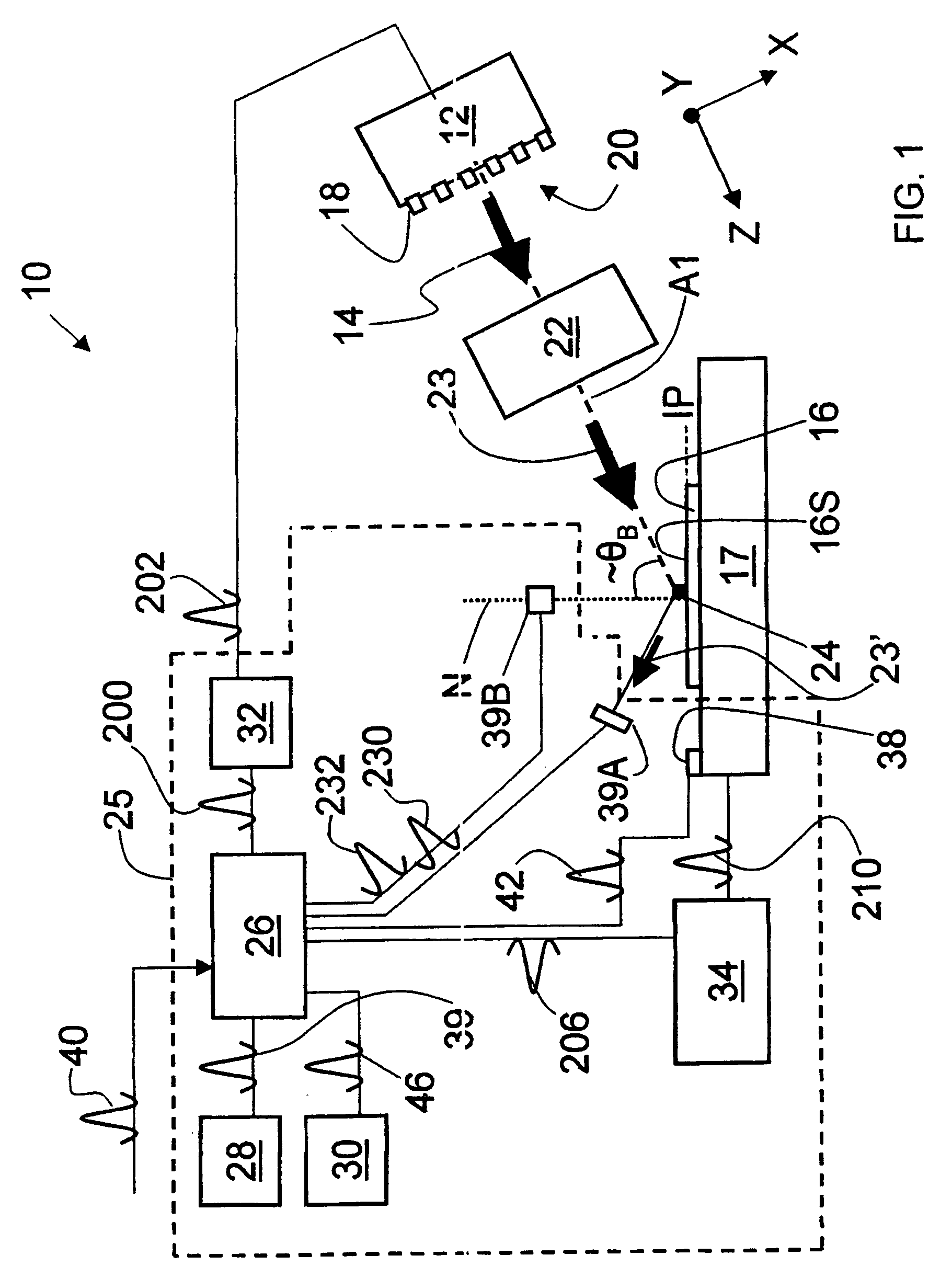
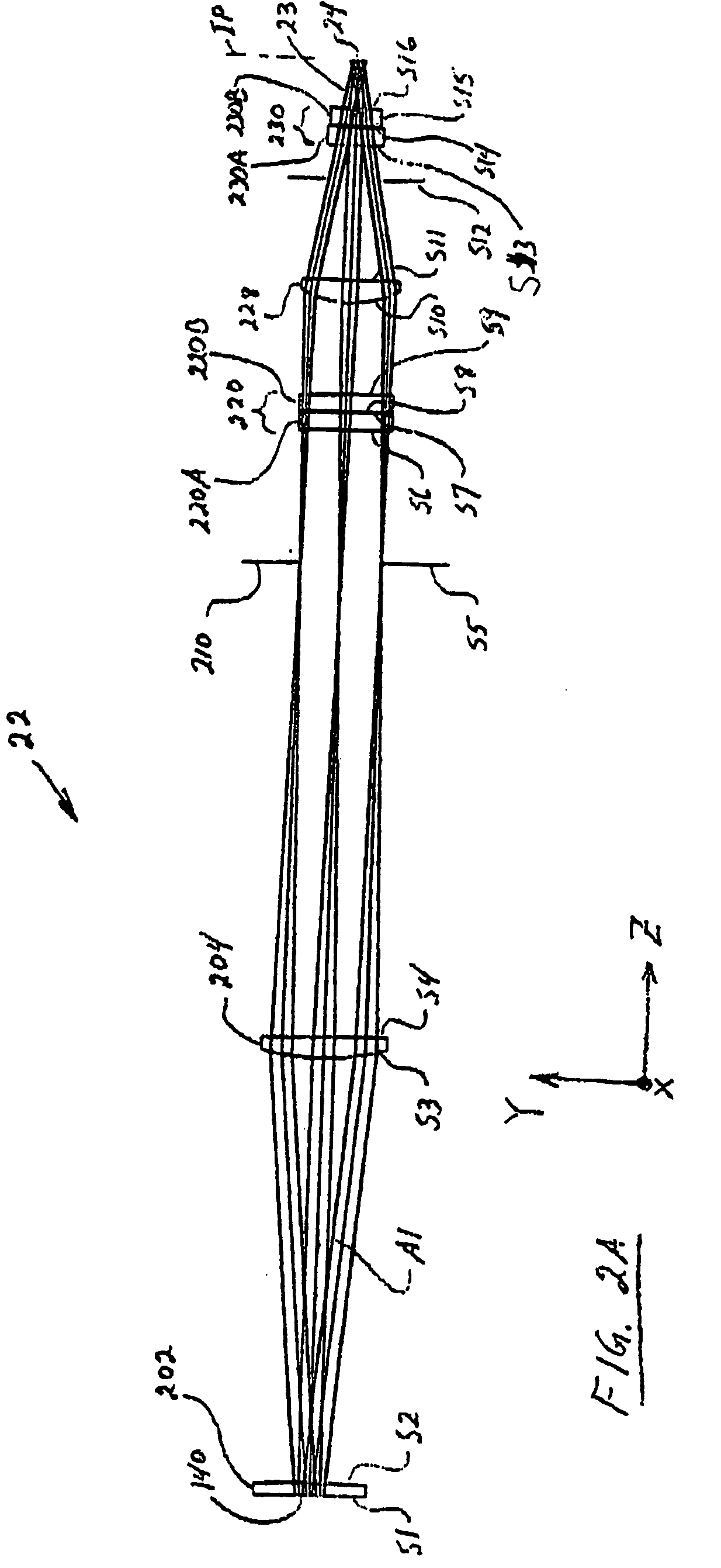
FIG. 1 is a schematic diagram of an example embodiment of the LTP apparatus 10 in accordance with the present invention. The apparatus 10 includes a two-dimensional laser diode array 12 and that generates relatively intense radiation 14 used for treating (i.e., irradiating) a substrate 16 supported by a movable stage 17. The substrate surface 16S resides at or near an image plane IP of an LTP optical system 22. These elements as well as others making up apparatus 10 are discussed separately below.

Laser Diode Array 12

Laser diode array 12 includes a plurality of laser diodes 18 positioned at regularly spaced intervals along a two-dimensional emission face 20 of the array. In an example embodiment, laser diode array 12 is formed by combining (e.g., “stacking”) linear diode arrays that make u...


PUM

PropertyMeasurementUnit
wavelengthsaaaaaaaaaa
Brewster's angleaaaaaaaaaa

Abstract

A method and apparatus for performing laser thermal processing (LTP) using a two-dimensional array of laser diodes to form a line image, which is scanned across a substrate. The apparatus includes a two-dimensional array of laser diodes, the radiation from which is collimated in one plane using a cylindrical lens array, and imaged onto the substrate as a line image using an anomorphic, telecentric optical imaging system. The apparatus also includes a scanning substrate stage for supporting a substrate to be LTP processed. The laser diode radiation beam is incident on the substrate at angles at or near the Brewster's angle for the given substrate material and the wavelength of the radiation beam, which is linearly P-polarized. The use of a two-dimensional laser diode array allows for a polarized radiation beam of relatively high energy density to be delivered to the substrate, thereby allowing for LTP processing with good uniformity, reasonably short dwell times, and thus reasonably high throughput.

Description

BACKGROUND OF THE INVENTION 1. Field of the Invention The present invention relates to laser thermal processing, and in particular relates to apparatus and methods for performing laser thermal processing with laser diode radiation. 2. Description of the Prior Art Laser thermal processing (“LTP”) (also referred to as “laser thermal annealing”) is a technique used to anneal and / or activate dopants of source, drain or gate regions of integrated devices or circuits, to form silicide regions in integrated devices or circuits, to lower contact resistances of metal wiring coupled thereto, or to trigger a chemical reaction to either deposit or remove substances from a substrate. Various devices for performing LTP of a semiconductor substrate have been known and used in the integrated circuit (IC) fabrication industry. LTP is preferably done in a single cycle that brings the temperature of the material being annealed up to the annealing temperature and back down in a single cycle. If a ...

Claims


Application Information

Patent Timeline
Patent Type & Authority Applications(United States)
IPC IPC(8): B23K26/00B23K26/06B23K26/073G03BH01L21/20
CPCB23K26/0604B23K2201/40B23K26/073B23K2101/40
Inventor TALWAR, SOMITMARKLE, DAVID A.
Owner VEECO INSTR
Why Eureka
Try Eureka