Eureka AIR delivers breakthrough ideas for toughest innovation challenges, trusted by R&D personnel around the world.

Semiconductor laser device and optical disc drive

a semiconductor laser and optical disc technology, applied in semiconductor lasers, laser details, electrical devices, etc., can solve the problems of short device life, difficult to surely obtain good ingaasp crystals under this condition, and affecting reliability, so as to achieve high-reliability semiconductor laser devices, the effect of preventing degradation of the strained quantum well active region and sufficiently reducing the temperature of spinodal decomposition

Inactive Publication Date: 2005-02-24
SHARP FUKUYAMA LASER CO LTD
View PDF3 Cites 4 Cited by
  • Summary
  • Abstract
  • Description
  • Claims
  • Application Information

AI Technical Summary

Benefits of technology

According to the above constitution, the strain of the InGaAs1-xPx well layer with respect to the GaAs substrate becomes a compressive strain of less than 1%, and the P composition in Group V elements becomes smaller than 0.55. Thus, the temperature of the spinodal decomposition is sufficiently decreased to an extent for growing InGaAsP, so that a highly reliable semiconductor laser device is obtained. Further, the well layer is made aluminum-free whereby degradation of the strained quantum well active region is prevented. Furthermore, since the strain of the well layer is a compressive strain of less than 1%, it becomes possible to more decrease the threshold current density compared with the case of no strain.
According to the embodiment, since the well layer has a layer thickness larger than 8 nm, the average strain amount within the active region becomes smaller. This tendency is true even if the compressive strain amount of the well layer and the tensile strain amount of the barrier layer are set in such a manner as to have a big difference in absolute value therebetween for the purpose of enlarging energy band difference. Accordingly, it becomes possible to simultaneously achieve both the low threshold current and high reliability. Furthermore, even if dullness occurs in steepness of the interface between the well layer and the barrier layer, the effect of the dullness in the energy band structure is relatively reduced. Thus, deterioration of the characteristics of the element due to the dullness of the energy band structure is prevented.

Problems solved by technology

However, this structure of the semiconductor laser devices has a serious problem regarding reliability such as Catastrophic Optical Damage (COD) or the short lifetime of the device because the active layer contains aluminum (Al).
Thus, it is difficult to surely obtain good InGaAsP crystals under this condition.
However, as mentioned above, the tensile strain of 1% cannot be obtained within the range of the region (a) of the Eg required for the InGaAsP well layer(s) in the case of the semiconductor laser device having the InGaAsP well layer(s) that oscillates laser light at the conventional wavelength of 780 nm.
That is, there is a problem that a low threshold current cannot be obtained in the case where a semiconductor laser device having a well layer(s) with a tensile strain is oscillated at a wavelength of 780 nm.

Method used


Image

  • Semiconductor laser device and optical disc drive
  • Semiconductor laser device and optical disc drive
  • Semiconductor laser device and optical disc drive

Examples


first embodiment

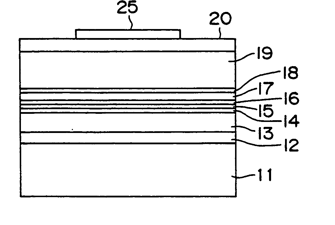
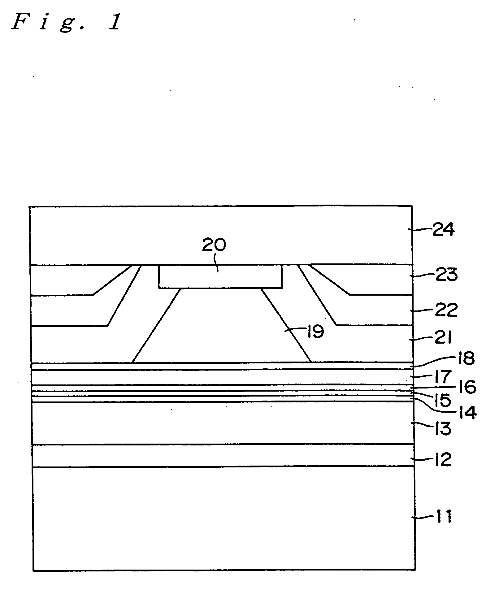
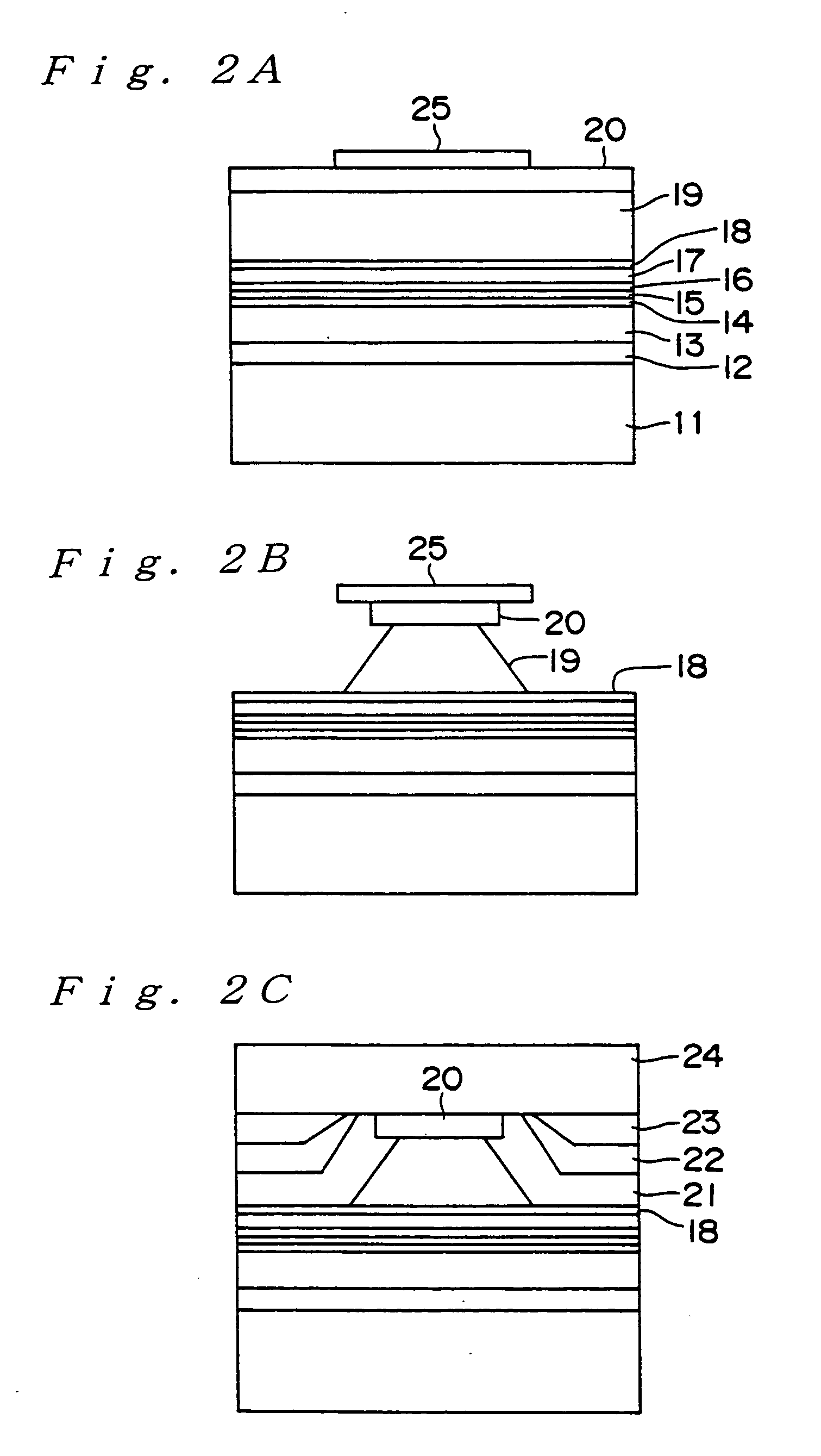
FIG. 1 is a cross sectional view showing a constitution in a semiconductor laser device of the present embodiment. FIG. 2 is a schematic cross sectional view showing a process for producing the semiconductor laser device shown in FIG. 1. The present embodiment relates to a semiconductor laser device whose oscillation wavelength belongs to a 0.78-μm band, the semiconductor laser device having a quantum well active region made of InGaAsP well layers and having a compressive strain of larger than 0.25 and smaller than 1.0%.

As shown in FIG. 1, in the semiconductor laser device of the present embodiment, the following layers are sequentially formed on an n-type GaAs substrate 11: an n-type GaAs buffer layer (layer thickness of 0.5 μm) 12, an n-type Al0.5Ga0.5As lower cladding layer (layer thickness of 1.7 μm) 13, a lower light-guiding layer 14 consisting of two layers of an i-type Al0.3Ga0.7As (layer thickness of 40 nm) and an i-type Al0.2Ga0.8As (layer thickness of 5 nm) sequentially ...

second embodiment

FIG. 5 is a cross sectional view showing a constitution of a semiconductor laser device of the second embodiment. In the semiconductor laser device of the present embodiment, as shown in FIG. 5, on an n-type GaAs substrate 31, there are sequentially stacked an n-type GaAs buffer layer (layer thickness of 0.5 μm) 32, an n-type Al0.4Ga0.6As lower first cladding layer (layer thickness of 1.5 μm) 33a, an n-type Al0.5Ga0.5As lower second cladding layer (layer thickness of 1.5 μm) 33b, an i-type Al0.35Ga0.65As lower light-guiding layer (layer thickness of 30 nm) 34, a multiquantum well active region (oscillation wavelength of 0.78 μm) 35, an i-type Al0.35Ga0.65As upper light-guiding layer (layer thickness of 30 nm) 36, a p-type Al0.5Ga0.5As upper first cladding layer (layer thickness of 0.2 μm) 37, a p-type GaAs etching stopper layer (layer thickness of 3 nm) 38, a p-type Al0.5Ga0.5As upper second cladding layer (layer thickness of 1.2 μm) 39 and a p-type GaAs contact layer (layer thickne...

third embodiment

FIG. 6 is a cross sectional view showing a constitution in a semiconductor laser device of the third embodiment. As shown in FIG. 6, in the semiconductor laser device of the present embodiment, on an n-type GaAs substrate 51, there are sequentially stacked an n-type GaAs buffer layer (layer thickness of 0.5 μm) 52, an n-type Al0.4Ga0.6As lower first cladding layer (layer thickness of 1.3 μm) 53a, an n-type Al0.5Ga0.5As lower second cladding layer (layer thickness of 1.0 μm) 53b, a lower light-guiding layer 54 consisting of two layers of an i-type Al0.35Ga0.65As (layer thickness of 30 nm) and an i-type Al0.25Ga0.75As (layer thickness of 3 nm) in this order, a multiquantum well active region (oscillation wavelength of 0.78 μm) 55, an upper light-guiding layer 56 consisting of two layers of an i-type Al0.25Ga0.75As (layer thickness of 3 nm) and an i-type Al0.35Ga0.65As (layer thickness of 30 nm) in this order, a p-type Al0.5Ga0.5As upper first cladding layer (layer thickness of 0.2 μm)...


PUM


Abstract

A 780 nm band semiconductor laser device has an InGaAsP well layer, phosphorous composition of which is 0.51 smaller than 0.55 to prevent spinodal decomposition in growing InGaAsP. A compressive strain of 0.65% less than 1% and more than 0.25% is introduced into the well layer to reduce threshold current thereof. Thus, the 0.78-μm band semiconductor laser device having the InGaAsP well layer stably operates for a long time even in outputting a high optical power of 100 mW or more. A tensile strain of 1.2% is also introduced into barrier layers within the active region so as to compensate the stress due to the compressive strain of the well layer. As a result, the reliability of the semiconductor laser device is further increased during a high output operation.

Description

TECHNICAL FIELD This invention relates to a semiconductor laser device used for an optical disc unit in the field of CD (compact disc), MD (mini disc) or the like, wherein a particularly high optical power has recently been required, and relates to an optical disc unit using the semiconductor laser device. BACKGROUND ART AlGaAs semiconductor laser devices are abundantly used for various purposes such as light-emitting devices for pickup in the field of optical discs including CD, MD or the like. In general, the semiconductor laser devices have a structure formed by sequentially stacking, for example, an n-type AlGaAs cladding layer, an AlGaAs active layer, a p-type AlGaAs cladding layer and a p-type GaAs contact layer in this order on an n-type GaAs substrate. However, this structure of the semiconductor laser devices has a serious problem regarding reliability such as Catastrophic Optical Damage (COD) or the short lifetime of the device because the active layer contains aluminum ...

Claims


Application Information

Patent Timeline
Patent Type & Authority Applications(United States)
IPC IPC(8): H01S5/223H01S5/343
CPCB82Y20/00H01S5/2231H01S2302/00H01S5/34373H01S2301/00H01S5/3434
Inventor FUJISHIRO, YOSHIEOHBAYASHI, KENYAMAMOTO, KEI
Owner SHARP FUKUYAMA LASER CO LTD
Why Eureka
Eureka Blog
Learn More