Semiconductor fabrication process, lateral PNP transistor, and integrated circuit
- Summary
- Abstract
- Description
- Claims
- Application Information
AI Technical Summary
Benefits of technology
Problems solved by technology
Method used
Image
Examples
Embodiment Construction
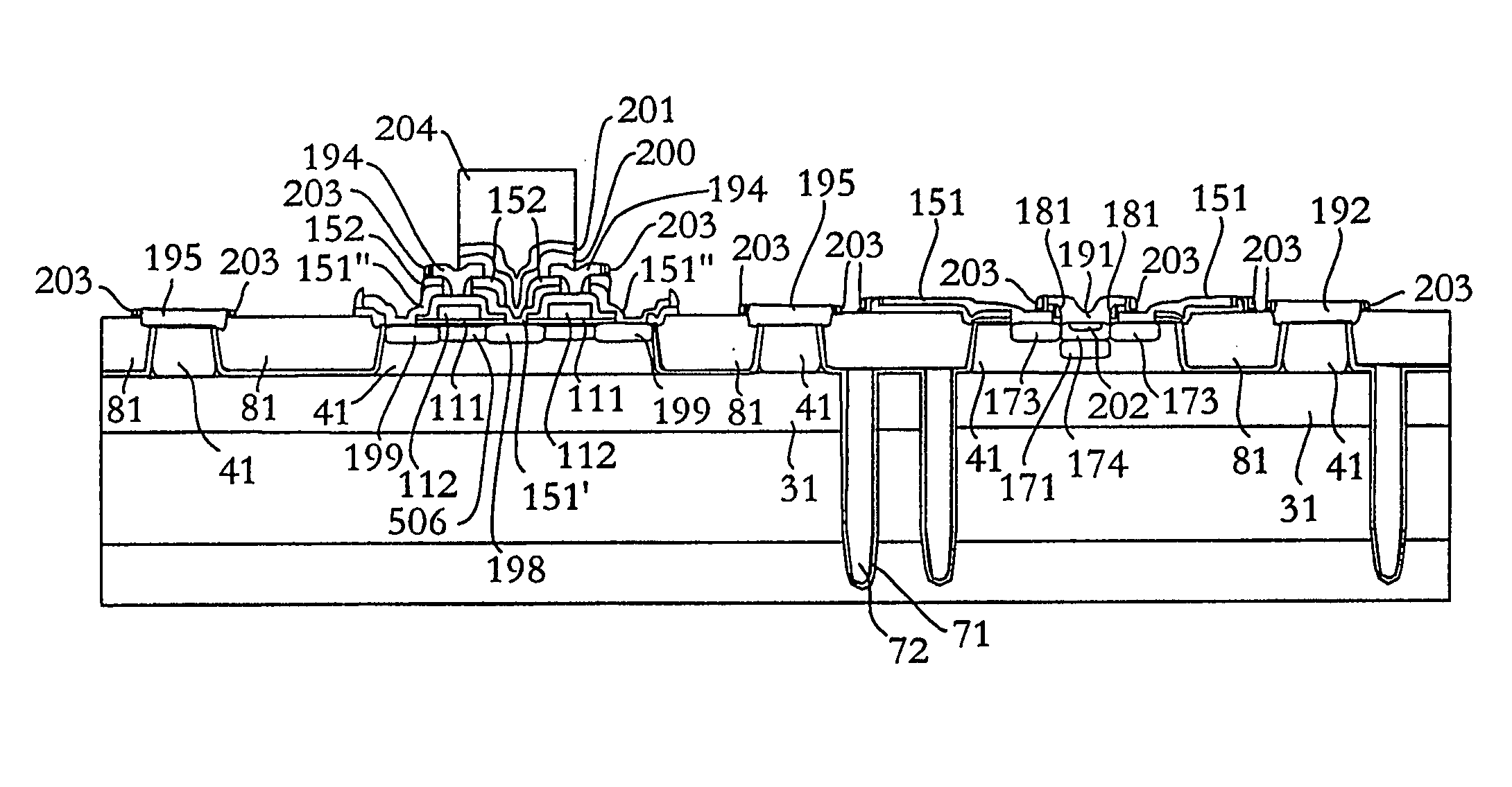
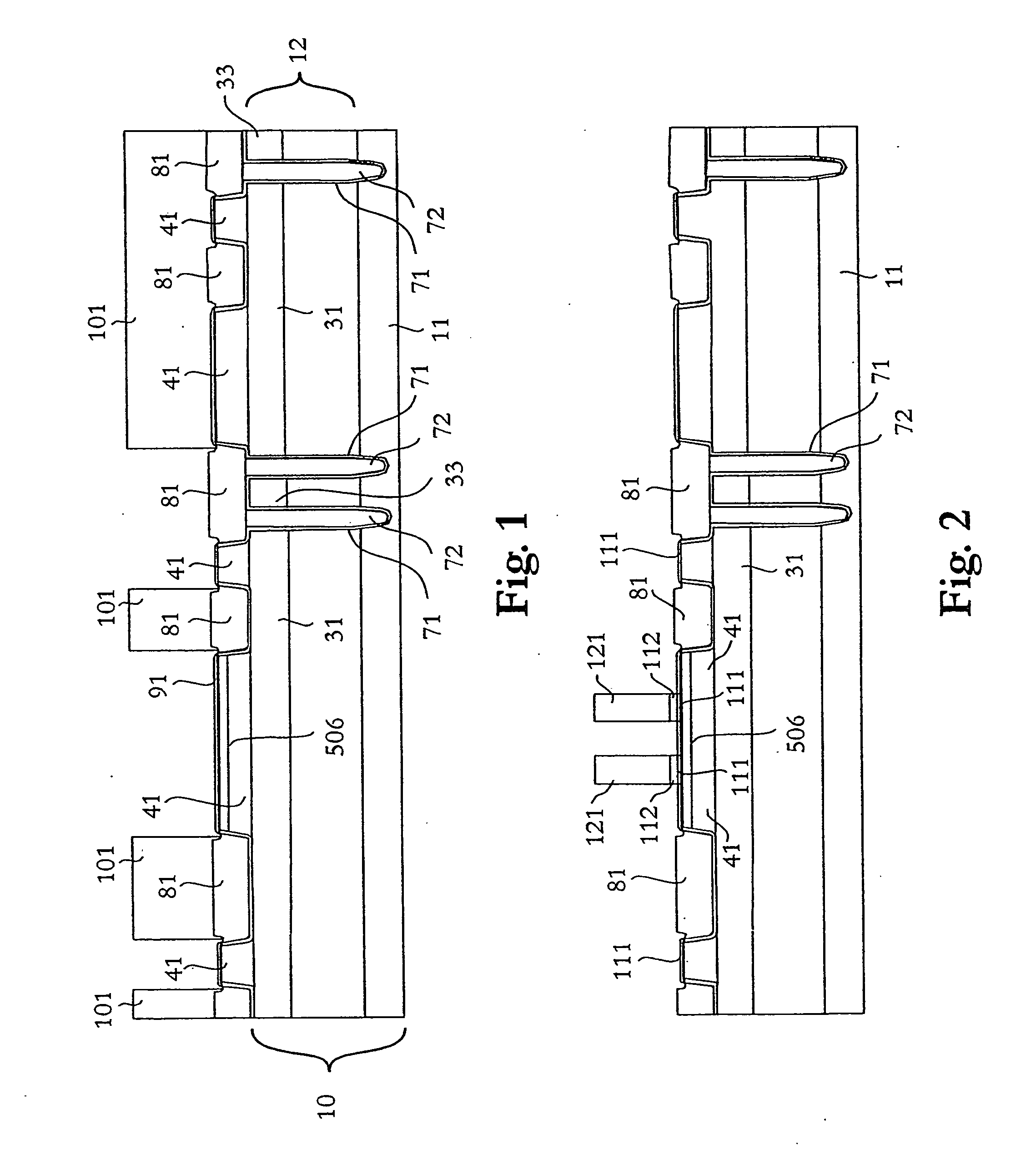
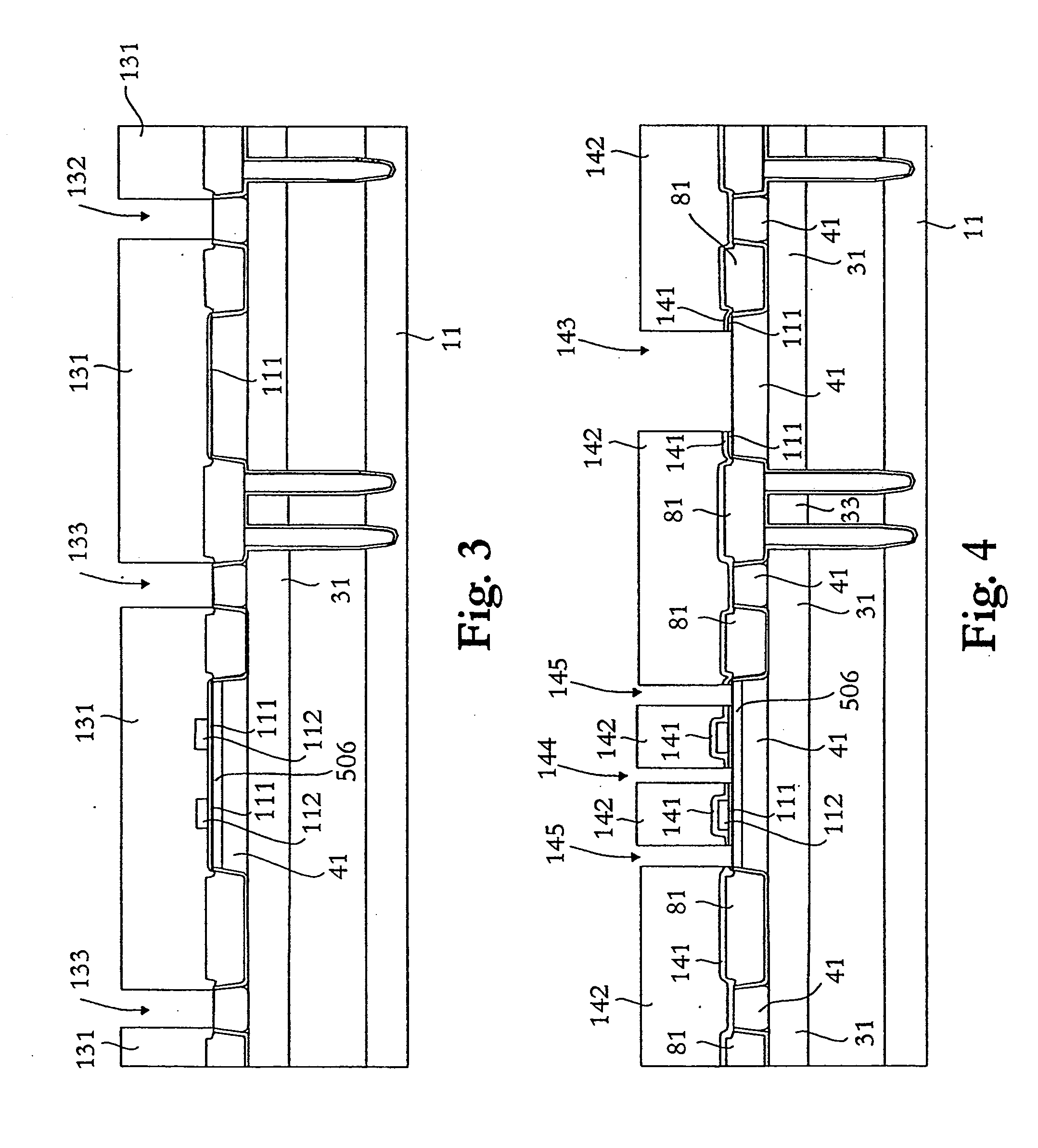
[0029] A process of manufacturing a PMOS-based lateral PNP transistor in a bipolar process, to which only a few process steps are added, is described below. To illustrate the process, a description of simultaneous formation of a vertical bipolar NPN transistor is also included.
[0030] To reach a structure as the one illustrated in FIG. 1 a starting material 10 consisting of a highly p+-doped wafer 11 is provided, on which a low-doped silicon layer 12 of p-type is grown. Alternatively, the p-type wafer can be a homogeneously low-doped p-type wafer (not illustrated).
[0031] In the surface layer 12 buried n-doped 31 and p-doped 33 regions are formed by means of (i) forming a thin protective layer of silicon dioxide on the layer 12; (ii) forming a mask thereon by photolithographic methods to define areas for a PMOS structure, and the bipolar transistor, respectively; (iii) n+-type doping the areas defined by the mask; (iv) removing the mask; (v) heat treating the structure obtained; (vi...
PUM
 Abstract
Description
Claims
Application Information
 - R&D
- Intellectual Property
- Life Sciences
- Materials
- Tech Scout
- Unparalleled Data Quality
- Higher Quality Content
- 60% Fewer Hallucinations
Browse by: Latest US Patents, China's latest patents, Technical Efficacy Thesaurus, Application Domain, Technology Topic, Popular Technical Reports.
© 2025 PatSnap. All rights reserved.Legal|Privacy policy|Modern Slavery Act Transparency Statement|Sitemap|About US| Contact US: help@patsnap.com


