
Active removal of aliasing frequencies in a decimating structure by changing a decimation ratio in time and space

a decimating structure and time and space technology, applied in the field of wireless communication systems, can solve the problems of difficult integration of analog circuit components into integrated circuits, interference and/or noise added to sample streams, and complex filters such as anti-aliasing filters, which are difficult to design and integrate onto integrated circuits, etc., to achieve the effect of active detection and elimination and/or avoidance of aliasing frequency components, additional power consumption, and improved efficiency

Inactive Publication Date: 2005-02-03
TEXAS INSTR INC
View PDF2 Cites 33 Cited by
  • Summary
  • Abstract
  • Description
  • Claims
  • Application Information

AI Technical Summary

Benefits of technology

The present invention provides a number of advantages. For example, use of a preferred embodiment of the present invention permits active detection and elimination and / or avoidance of aliasing frequency components. Active detection and elimination and / or avoidance of aliasing frequency components allow the present invention to detect an aliasing frequency that was heretofore undetected or unexpected. The aliasing frequency can then be eliminated or avoided.
Also, use of a preferred embodiment of the present invention requires no additional hardware, such as an anti-aliasing filter. Analog anti-aliasing filters require a large amount of real estate on an integrated circuit and are expensive due to the precise values of their components. Digital anti-aliasing filters require additional processing power from a digital signal processor to implement and additional processing power requires additional power consumption and heat dissipation. By not requiring any additional hardware, use of a preferred embodiment of the present invention saves on both the real estate and the power consumption of the integrated circuit.
Additionally, use of a preferred embodiment of the present invention allows the detection of interferers and in lightly loaded systems, it is possible to avoid the interferers by shifting operating frequencies rather than having to actively eliminate the interferer.

Problems solved by technology

Unfortunately, analog circuit components, especially components such as capacitors, inductors, resistors, etc. necessary for the analog filters are difficult to integrate into an integrated circuit.
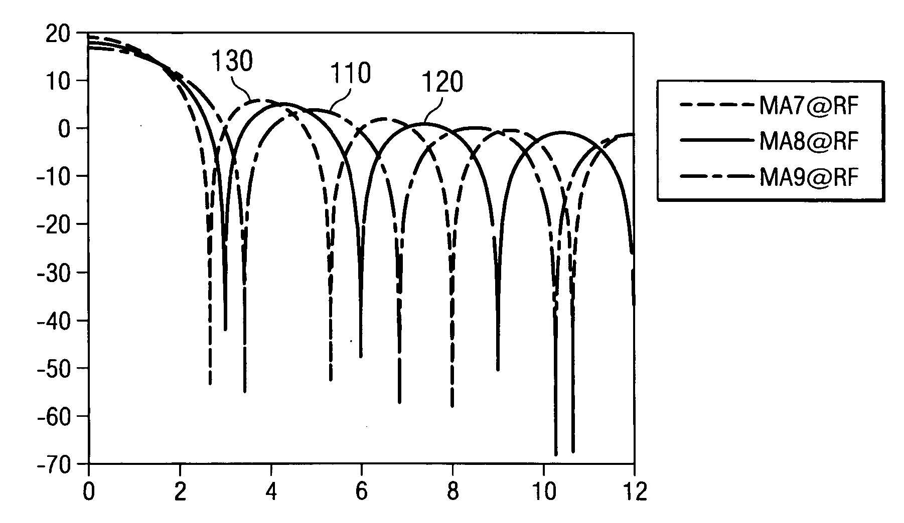
When the signal being sampled has frequency components at frequencies greater than one half of the Nyquist rate, these frequency components are aliased down into the signal and as a result, interference and / or noise is added to the sample stream.
However, anti-aliasing filters may be rather complex filters that are difficult to design and integrate onto an integrated circuit.
They can be difficult to design if the desired frequency response is sharp.
Furthermore, they can be both bulky (consuming a large amount of real estate) and expensive (due to requirements for precise component values).
In integrated circuits, it is often not possible to include an anti-aliasing filter on the same integrated circuit containing the sampling circuit and digital circuitry, therefore these filters may be external to the integrated circuit.
This requires that the signals go off-chip, reducing the overall performance of the system and introducing additional complexity.
Additionally, anti-aliasing filters are static in nature, meaning that their frequency response is set when they are designed and fabricated and cannot be changed to meet changing spectral environments; For example, should operating-conditions change such that a formerly low-powered, frequency component that was aliasing into a band of interest but had been previously ignored due to its low power, now for some reason becomes a significant source of interference, a static anti-aliasing filter will not be able to adapt to eliminate that particular aliasing frequency component.

Method used


Image

  • Active removal of aliasing frequencies in a decimating structure by changing a decimation ratio in time and space
  • Active removal of aliasing frequencies in a decimating structure by changing a decimation ratio in time and space
  • Active removal of aliasing frequencies in a decimating structure by changing a decimation ratio in time and space

Examples


Embodiment Construction

The making and use of the various embodiments are discussed below in detail. However, it should be appreciated that the present invention provides many applicable inventive concepts, which can be embodied in a wide variety of specific contexts. The specific embodiments discussed are merely illustrative of specific ways to make and use the invention, and do not limit the scope of the invention.

The following discussion focuses on a particular type of radio receiver mixer and its circuitry that is operating in a 2.4 Gigahertz frequency band and is adherent to the Bluetooth technical standards. The Bluetooth technical standard specifies a short-range wireless communications network whose intended purpose is a low-power and low-cost replacement for physical cabling. The Bluetooth technical standard is specified in a document entitled “Specification of the Bluetooth System, Version 1.1, Feb. 22, 2001,” which is incorporated herein by reference. While the discussion focuses on Bluetooth...


PUM


Abstract

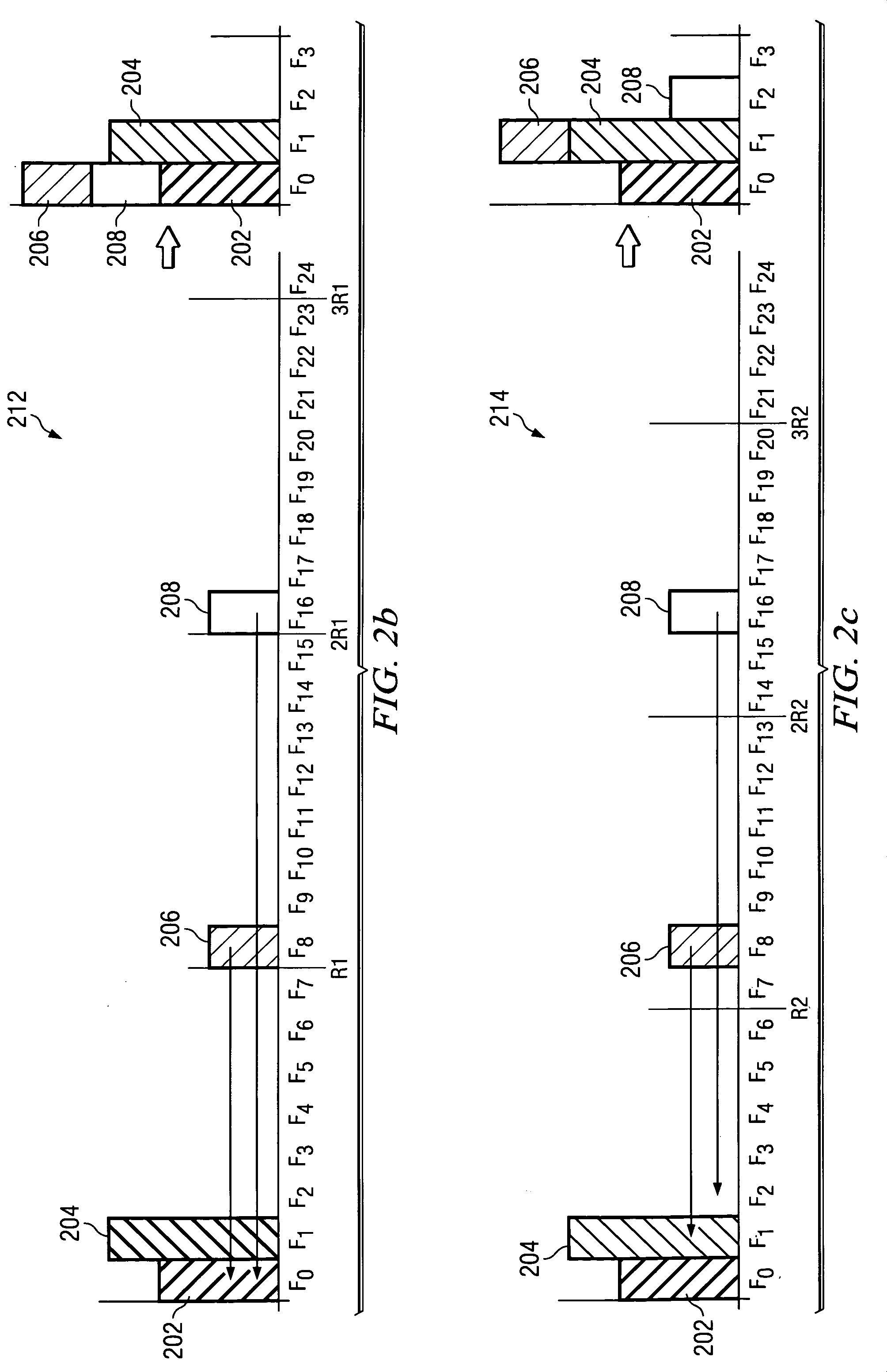
When a sample stream is decimated, frequency components from outside of a desired frequency band are aliased into the desired band, causing interference and loss of information. Different decimating ratios result in different frequencies aliasing into the desired frequency band. A current-mode sampling mixer 800 with capacitor banks 811 and 812 that are controlled by a digital control unit 820 with a capability to integrate and decimate an RF current at different decimating ratios is able to measure the frequency spectrum with different decimating ratios. The measured frequency spectrum is then analyzed to detect the presence of interferers aliased into the desired frequency band. The interferers can then be eliminated or avoided.

Description

FIELD OF THE INVENTION This invention relates generally to wireless communications systems and particularly to actively detecting and avoiding and / or removing aliasing frequency components using a configurable decimating ratio. BACKGROUND OF THE INVENTION Direct RF is a newly emerging field in wireless digital communications wherein analog RF signals that are transmitted over-the-air are directly sampled into a digital data stream suitable for digital signal processing. A typical wireless digital communications device would use analog filters, duplexors, mixers, analog-to-digital converters (ADC), etc. to convert the analog RF signals into a digital data stream that is suitable for digital signal processing. Unfortunately, analog circuit components, especially components such as capacitors, inductors, resistors, etc. necessary for the analog filters are difficult to integrate into an integrated circuit. This is especially true for the precise values of these components required fo...

Claims


Application Information

Patent Timeline
IPC IPC(8): H03D7/12H04B1/10
CPCH04B1/1036H03D7/125
Inventor MUHAMMAD, KHURRAMSTASZEWSKI, ROBERT B.FEYGIN, GENNADY
Owner TEXAS INSTR INC
Learn More