Method of measuring luminance of image display apparatus, method of manufacturing the same, method and apparatus for adjusting characteristics of the same

Inactive Publication Date: 2004-09-09
CANON KK
View PDF19 Cites 20 Cited by
  • Summary
  • Abstract
  • Description
  • Claims
  • Application Information

AI Technical Summary

Benefits of technology

[0029] Accordingly, it is an object of the present invention to provide a method of measuring luminance of an image display apparatus, a method of manufacturing the same, and a method and an apparatus for adjusting characteristics of the same, in which a time period required for measuring luminance of a pixel is reduced, and measuring accuracy is improved.

Problems solved by technology

However, there is a problem in that the multi-electron source including a number of electron-emitting devices arranged may cause some variations in electron-emitting characteristics of the individual electron-emitting device due to variations in process, and thus when it is applied to a large flat image display apparatus. variations in characteristics of the respective electron-emitting devices may result in variations in luminance.
The possible reasons why the electron-emitting characteristics of the electron-emitting devices in the multi-electron source differ from each other may be various causes such as variations in component of the material used for an electron-emitting section, tolerance of dimensions and configurations of each member of the device, non-uniform energizing condition in the energization forming process, and non-uniformity in energizing conditions or ambient gas In the energization activation process.
In order to remove all these causes, highly advanced manufacturing equipment or very strict process control are required, and satisfying these requirements involves huge manufacturing costs, which is not practical.
However, it was not sufficient in the following reasons.
The process of measuring the characteristics of the device above has a problem in that when applied to an image display apparatus having a large number of pixels such as a high-resolution image display apparatus including a prevailing high quality TV, time period required for performing these steps increases, which results in lowering of productivity.
In addition, measurement of luminance of each pixel may result in considerable lowering of accuracy of measurement of luminance signal of the device to be measured due to the influence from the adjacent devices, such as color mixture, caused by misalignment of the fluorescent material or displacement of irradiating position of electron beams.
In addition, accuracy of measurement was not sufficient.

Method used


Image

  • Method of measuring luminance of image display apparatus, method of manufacturing the same, method and apparatus for adjusting characteristics of the same
  • Method of measuring luminance of image display apparatus, method of manufacturing the same, method and apparatus for adjusting characteristics of the same
  • Method of measuring luminance of image display apparatus, method of manufacturing the same, method and apparatus for adjusting characteristics of the same

Examples


first embodiment

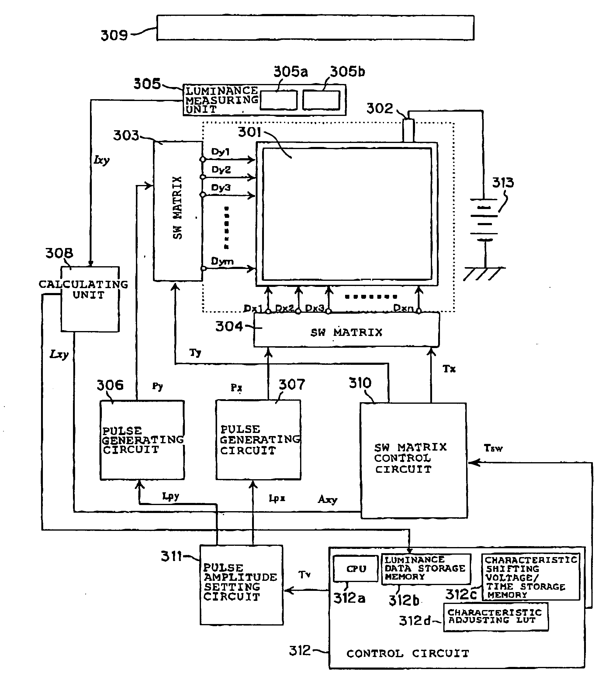
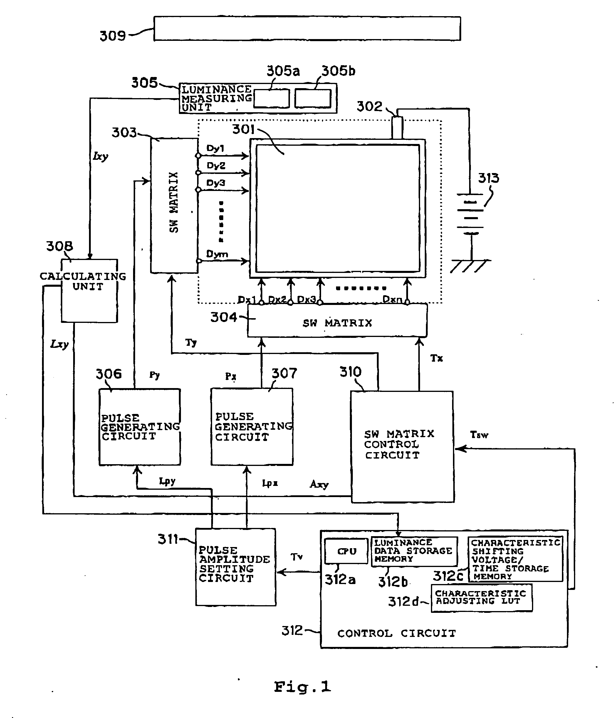
[0161] The electron-emitting oharacteristics of the image display apparatus fabricated in the same manner as that described above other than the point the adjacent electron-emitting devices are selected instead of the procedure in the first embodiment were adjusted.

[0162] As a consequence, points where partial display performance is deteriorated were found in the area. When having observed those points, they were the areas where the light-emitting points were superimposed at several adjacent portions.

[0163] It is easy to understand that there may be difference between the quality of image displayed in the case of the comparative example and the quality of image in the case where the "devices that are not adjacent to each other" are selected as in the first embodiment by supposing that another light-emitting point exists between two light-emitting points 501 in FIG. 5.

second embodiment

[0164] While the case in which pixels that are not adjacent to each other are selected and illuminated simultaneously for measuring luminance of the pixels has been described in the first embodiment a case in which the "pixels that are not adjacent to each other" to be selected are the same color selected from the three primary colors (red R. green G. and blue B) will be described in this embodiment.

[0165] Since the basic construction and the operation are the same as in the first embodiment, the description will not be made again.

[0166] In the method of measuring luminance in the first embodiment, the object to be measured was a color image display apparatus having a pixel constructions in which the pixels displaying R, G, and B are disposed adjacently with respect to each other, and those pixels were illuminated in a time-sharing manner for each of R, G and B so that the devices that are not adjacent to each other were simultaneously selected. Then the characteristic adjustment wa...

third embodiment

[0178] In this embodiment, when selecting the devices to be driven and measured in the first embodiment, the devices that were not adjacent to each other in a certain row and a plurality of rows that were not adjacent to each other were selected simultaneously, and were illuminated separately for R, G, and B for measuring luminance.

[0179] When the characteristics were adjusted in the same manner as the second embodiment except for the point described above, the same image display as in the second embodiment was achieved,

[0180] According to this embodiment, since the tolerance of accuracy of alignment of measuring equipment and of panel dimensions could be widened, and correction of sensitivity of the measuring equipment could be achieved at once, the measuring operation could advantageously be simplified.


PUM


Abstract

A method of measuring luminance of an image display apparatus, a method of manufacturing the same, and a method and an apparatus for adjusting characteristics of the same, in which accuracy of measurement is improved while reducing time for measuring luminance of a pixel are provided. A plurality of devices that are not adjacent to each other (for example the devices of the same color out of R, G, and B) are selected and illuminated simultaneously, and luminance is measured for each of them. Based on measured luminance, the electron-emitting characteristics of the respective electron-emitting device as are adjusted based on measured luminance.

Description

[0001] This application claims the right of priority under 35 U.S.C. .sctn.119 based on Japanese Patent Application No(s). JP2002-218204, filed on Jul. 26, 2002 and JP 2003-279137 filed on Jul. 24, 2003 which are hereby incorporated by reference herein their entirety as if fully set forth herein.[0002] 1. Field of the Invention[0003] The present invention relates to a method of measuring luminance of an image display apparatus, a method of manufacturing the same, and a method and an apparatus for adjusting characteristics of the same, for adjusting luminance of pixels provided in the image display apparatus.[0004] 2. Description of the Related Art[0005] In the related art, as a method of inspecting luminance of an image display apparatus, a method of inspecting pixel of a liquid crystal panel using a linear sensor is disclosed in, for example, JP-UM-A-4-055535 (Document 2). In addition, in an image display apparatus employing a surface conduction electron-emitting device (hereinafte...

Claims


Application Information

Patent Timeline
IPC IPC(8): G01M11/00G01J1/42G02F1/13G09G3/00G09G3/22H01J9/42H01J9/44
CPCG09G3/006G09G2320/0285G09G3/22G02F1/13
Inventor YAMASHITA, MASATAKAYAMAGUCHI, EIJIYAMANO, AKIHIKO
Owner CANON KK
Why Eureka
Try Eureka