
Copper plating bath and plating method for substrate using the copper plating bath

a technology of copper plating and copper bath, which is applied in the direction of printed element electric connection formation, liquid/solution decomposition chemical coating, coating, etc., can solve the problems of difficult layering of copper plating over the holes, requiring a considerable period of time, and a third method is simple, but has a serious reliability problem

Inactive Publication Date: 2003-06-12
EBARA-UDYLITE CO LTD
View PDF2 Cites 60 Cited by
  • Summary
  • Abstract
  • Description
  • Claims
  • Application Information

AI Technical Summary

Benefits of technology

[0013] As a result of extensive studies on plating baths for a long period of time to solve the above-described problems, the inventors of the present invention have found that a copper plating bath containing certain components exhibits excellent via-filling characteristics and plating uniformity, can plate co-existing through-holes with superior plating uniformity, and can produce copper plating with high electric reliability on electric circuit boards such as semiconductor wafers having circuits patterns with minute wiring grooves, printed circuit boards, and the like, with an additional advantage of allowing easy analysis of major components of the plating bath.

Problems solved by technology

With via-hole plating, in which a metal film is formed on the side or bottom inside the via-holes, there are difficulties in layering a conductive layer over the holes.
Of these methods, the first method requires grinding of deposited copper plating layers having a substantial thickness, whereas the second method has a drawback of requiring a considerable period of time to obtain a copper plating layer with a desired thickness.
The third method is simple, but has a serious problem in terms of reliability.
Because this method employs a paste in which metals are dispersed using a solvent and the like, there are problems such as limited conductivity, formation of voids or shrinkage due to a reduction in volume after filling, and peeling of plate from the internal wall of the holes.
However, the plating solutions and plating methods heretofore proposed have the following drawbacks in practical use.
However, although this type of plating solution is suitable for a panel plating method for plating the entire surface of the substrates, the leveling component is easily affected by the thickness of the diffusion layer and the flow rate of the plating solution when applied to a substrate in which circuits are previously patterned by a resist or the like or a substrate with both patterns and through-holes.
As a result, the metal thickness significantly differs in the center or ends of vias or wires, or a metal may become thick only in the through-hole entrance corners or the one side of the through-hole internal walls, impairing reliability on laminated layers and electric properties.
Although a method of plating using a pulse wave-form has also been proposed, the method not only involves high cost for the facility which results in a high production cost, but also a problem of complicated electric current control.
Furthermore, conventional plating solutions result in difficulty in analysis and control due to inclusion of three or more components as additives.
The difficulty in analysis and control impairs dense filling properties, uniformity of film thickness in pattern plating, and maintenance of consistent properties, thereby significantly affecting the yield and cost of the products.
However, a huge amount of air must be supplied and discharged if the all amount of down-flow clean air depends on the outside source.
Plated copper film within the set cut width can be removed inasmuch as the rotation is above the limit, under which the amount of liquid leaking from the back to the surface causes problems.
Specifically, although grains are difficult to grow in thin wiring, wide wiring may allow growth of grains.
During the course of growth of grains in the annealing process, very minute pores which are difficult to observe even by an SEM (scanning electron microscope) are believed to move upwardly while flocculating, producing recesses for micro voids on the surface of the wires.

Method used


Image

  • Copper plating bath and plating method for substrate using the copper plating bath
  • Copper plating bath and plating method for substrate using the copper plating bath
  • Copper plating bath and plating method for substrate using the copper plating bath

Examples


example 1

[0206] Evaluation of via-Hole Filling Performance

[0207] A patterned substrate with a configuration as shown in FIG. 30, having blind via-holes with a diameter of 80 .mu.m and a depth of 40 .mu.m and a pad with a diameter of 150 .mu.m, and processed by electroless copper plating to provide electro conductivity was prepared. A LIZATRON process (Ebara-Udylite Co., Ltd.) was used for the electroless copper plating.

[0208] After the conductivity processing, the patterned substrate was plated with copper using the following seven copper plating baths (plating baths 1-4 of the present invention and comparative plating baths 1-3). Copper plating was carried out at 25.degree. C. and a cathode current density of 2 A / dm.sup.2 for 60 minutes with stirring by aeration.

[0209] Additives commonly used with printed circuit boards were used for the comparative plating baths 1 and 3. The comparative plating bath 1 has the same formulation as the plating bath of the present invention 1, except for the t...

example 2

[0216] Evaluation of Film Thickness Uniformity in Pad Wiring Area

[0217] A patterned substrate (line width: 100 .mu.m, depth: 30 .mu.m) shown in FIG. 32, modeling a package substrate used for MPU and the like was prepared. The patterned substrate was plated with copper using the plating bath 2 of the present invention and comparative plating bath 2 used in Example 1 under the same conditions as employed in Examples 1, to evaluate the film thickness uniformity in the wiring area.

[0218] The evaluation was carried out in the same manner as in Example 1 according to the section film thickness measurement method using a microscope. The plate thickness at two points, the line end (resist side) L.sub.1 and the center L.sub.2, shown in FIG. 33 was measured for evaluation of film thickness uniformity in the pad wiring area. The results are shown in Table 2.

[0219] (Results)

3 TABLE 2 L.sub.1 (.mu.m) L.sub.2 (.mu.m) L.sub.1 / L.sub.2 Plating bath 2 of the 25 24.5 1.02 present invention Comparative...

example 3

[0221] Through-Hole Throwing Power Evaluation

[0222] To investigate possibility of applying the plating baths of the present invention to through-hole plating based on the results of Examples 1 and 2, the following throwing power test in through-holes was carried out.

[0223] A substrate (FR-4) with a thickness of 1.6 mm in which through-holes with a diameter of 1 mm and 0.3 mm were bored was used as a sample. The sample was processed by electroless copper plating using the same LIZATRON process as used in Example 1 to form an electroless copper plate with a thickness of 0.5 .mu.m.

[0224] The through-holes of this substrate were plated using the plating bath 1 of the present invention and the comparative plating bath 2 at 25.degree. C., a current density of 2A / dm.sup.2for 70 minutes. For comparative evaluation, the same experiment was carried out using a conventional plating bath for through-holes (comparative plating bath 3).

[0225] Throwing power (%) was determined by measuring the pla...


PUM

PropertyMeasurementUnit
concentrationaaaaaaaaaa
chlorine concentrationaaaaaaaaaa

Abstract

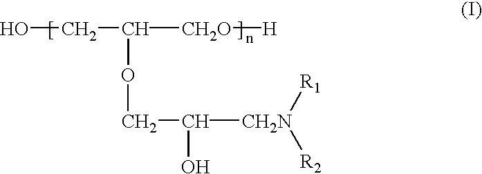
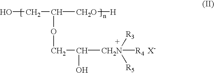
A copper plating bath comprising a reaction condensate of an amine compound and glycidyl ether and / or a quaternary ammonium derivative of this reaction, condensate, and a plating method using this copper plating bath are disclosed. A copper plating bath capable of providing highly reliable copper plating on a substrate such as a silicone wafer semiconductor substrate or printed board having minute circuit patterns and small holes such as blind via-holes, through-holes, and the like, and a method of copper plating using the copper plating bath can be provided.

Description

[0001] The present invention relates to a copper plating bath and a plating method for substrates using the copper plating bath. More particularly, the present invention relates to a copper plating bath capable of providing a highly reliable copper plating on a substrate such as a silicone wafer semiconductor substrate or printed board having minute circuit patterns and small holes such as blind via-holes, through-holes, and the like, and to a method of copper plating using the copper plating bath.DESCRIPTION OF BACKGROUND ART[0002] Recently, a build-up method is being applied to mounting circuits for electronic equipment such as cellular phones, personal computers, videos, game machines, and the like. In the build-up method, small holes such as through-holes and via-holes are provided through a laminated board, and metals are deposited in such small holes to allow interconnection among several different circuit layers, whereby multiplayer circuits are fabricated. Of these small hol...

Claims


Application Information

Patent Timeline
Patent Type & Authority Applications(United States)
IPC IPC(8): C25D3/38H05K3/42
CPCH05K3/423C25D3/38
Inventor HAGIWARA, HIDEKIKIMIZUKA, RYOICHITERASHIMA, YOSHITAKAMARUYAMA, MEGUMIMIYAKE, TAKASHINAGASAWA, HIROSHISAHODA, TSUYOSHIIIMURA, SEIJI
Owner EBARA-UDYLITE CO LTD
Learn More