Electron beam lithography

a technology of electron beams and lithography, applied in the field of electron beam lithography, can solve problems such as poor focus quality

Inactive Publication Date: 2003-01-30
AVAGO TECH INT SALES PTE LTD
View PDF0 Cites 5 Cited by
  • Summary
  • Abstract
  • Description
  • Claims
  • Application Information

AI Technical Summary

Problems solved by technology

Likewise, when chromatic aberration only is taken into account, focus quality worsens due to a large fraction of slow electrons in the beam.

Method used


Image

  • Electron beam lithography
  • Electron beam lithography
  • Electron beam lithography

Examples


Embodiment Construction

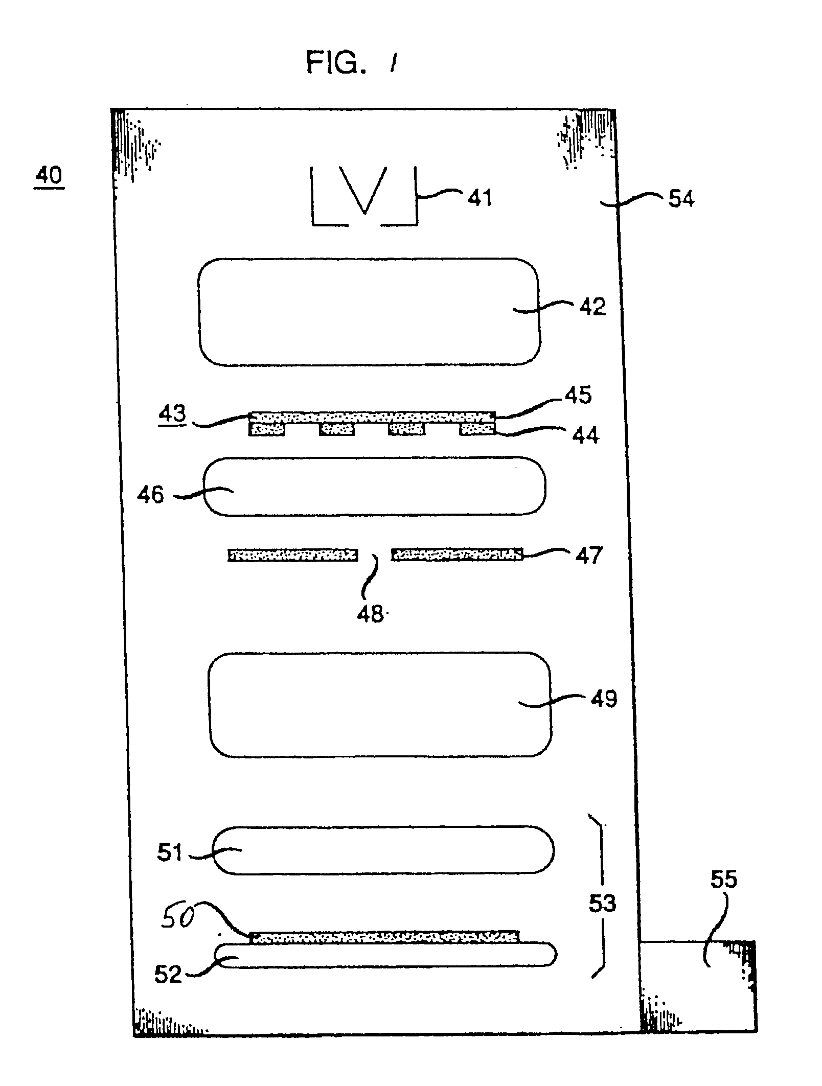
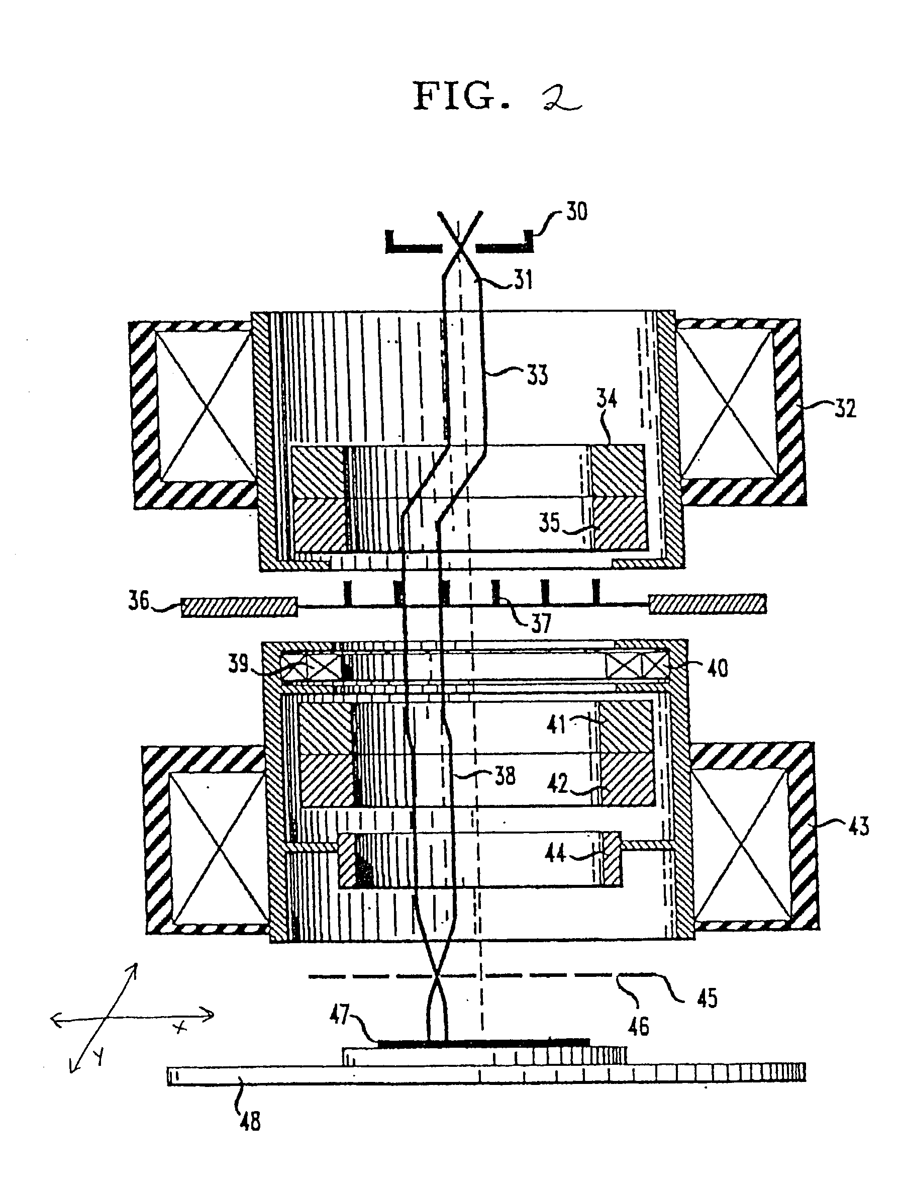
[0039] FIG. 11 illustrates an exemplary embodiment of an electron patterning system 100 of the present invention in one embodiment. The electron patterning system 100 may include a gun 102, a first lens system 104 (with an optical shaping aperture 106 at mid-plane), a blanking aperture 108, a second lens system 110, a mask 112, a projection doublet 114, including two lenses 116, 118 and a back focal plane 117 (with aperture 117a), and a wafer 120. FIG. 12 illustrates the mask 112, the projection doublet 114, and a wafer 120 in more detail. In particular, the lens 116 may include a magnetic shell 122, windings 124, and at least one deflector 126. An aperture 128 may be placed between the two lenses 116, 118. FIG. 12 also illustrates the relationship between the sub-field at the mask 112 and the sub-field at the wafer 120.

[0040] As discussed above with respect to FIG. 5, the goal is to place the wafer 120 of FIG. 11 in the plane where the image will be best focused. As outlined above,...


PUM

PropertyMeasurementUnit
thickaaaaaaaaaa
chromatic aberrationsaaaaaaaaaa
thicknessaaaaaaaaaa

Abstract

An apparatus and method of focusing including a source for producing an electron beam, a mask and a projection column, through which the electron beam passes, and a wafer on which the electron beam is to be focused. The wafer is located in a plane where spherical aberrations of the projection column reduce the negative defocusing effect caused by chromatic aberrations in the projection column. The apparatus and method are applicable to general electron patterning tools, electron patterning tools where a thickness of the mask is smaller than an electron mean free path of the electron patterning tool, and the SCALPEL(TM) electron patterning tool.

Description

[0001] 1. Field of the Invention[0002] The invention is generally directed to electron patterning, and more particularly electron patterning using scatter-nonscatter masking and even more particularly electron patterning in accordance with the SCALPEL process described in U.S. Pat. No. 5,079,112, issued Jan. 7, 1992. The present invention is also applicable to ion patterning.[0003] 2. Description of the Related Art[0004] An exemplary conventional apparatus 40 depicted in FIG. 1 includes an electron or other energy source 41, condenser lens system 42, mask 43 including blocking regions 44 and transparent regions 45, objective lens 46, back focal plane filter 47 shown as provided with on-axis aperture 48, projector lens system 49, exposure medium 50, between lens 51 and stage 52, which together constitute registration and alignment system 53. The apparatus 40 is completed by vacuum chamber 54 and air lock 55, the latter providing the specimen exchange.[0005] Another conventional appar...

Claims


Application Information

Patent Timeline
Patent Type & Authority Applications(United States)
IPC IPC(8): G03F7/20G03F7/207G03F9/02H01J37/153H01J37/20H01J37/21H01J37/317H01L21/027
CPCB82Y10/00B82Y40/00H01J37/3174H01J2237/1534Y10S430/143H01L21/027
Inventor KATSAP, VICTORMUNRO, ERICROUSE, JOHN ANDREWWASKIEWICZ, WARREN K.ZHU, XIEQING
Owner AVAGO TECH INT SALES PTE LTD
Why Eureka
Try Eureka