System and method for optimizing a lithography exposure process

a lithography exposure and optimization technology, applied in the field of semiconductor devices, can solve the problems of reducing system throughput, misalignment errors, and possible misalignment in lithographic processes, and achieve the effects of improving the quality of integrated circuit devices, reducing misalignment, and good quality alignmen

Active Publication Date: 2021-09-21
ONTO INNOVATION INC
View PDF45 Cites 1 Cited by
  • Summary
  • Abstract
  • Description
  • Claims
  • Application Information

AI Technical Summary

Benefits of technology

[0006]Correcting misalignment errors tends to negatively affect the throughput of a lithographic manufacturing process. Throughput relates to the rate at which die are produced by a process. Where time consuming misalignment corrections are undertaken on a continued basis, throughputs will drop. The reduction in throughput reduces the quantity of saleable product available. As a result, expected revenues will drop.
[0023]In one embodiment, the optimization of the creation of a recipe or set of instructions for lithographically exposing a substrate can be approached by fitting devices to a predetermined shot or by fitting shots to groups defined on the basis of alignment. The end goal is the same in either case, i.e. to obtain good quality alignments between a reticle and the devices in an efficient manner. In another embodiment of the present invention, alignment of a plurality of devices relative to a substrate of which they are part is determined. These devices are then grouped based on the determined alignment of the devices. This establishes a plurality of groups of devices, each device of the group having a similar alignment. Shots or arrays of lithographic patterns of various shapes and sizes are tiled, in the mathematical sense, over the plurality of groups of devices to define the shots for tiling each of the plurality of groups of devices with one or more arrays of lithographic patterns. A path is defined between each of the tiled patterns. The defined shots together with path establish a recipe for performing lithographic exposure of the devices. Once a recipe is in hand, the devices of the substrate are exposed according to the recipe to form at least a portion of a structure on the devices. One benefit of determining the alignment of the devices is that misalignment in the devices on the substrates may be used to correct or reduce subsequent misalignment of devices on a subsequent substrate that is being formed.

Problems solved by technology

However, during the semiconductor manufacturing process, misalignment in lithographic processes may occur.
These misalignment errors may be essentially random, e.g. the result of environmental factors such as temperature or atmospheric pressure change, or may be a result of systematic factors such as consistent positioning errors associated with a the pick and place system.
Misalignment errors in lithographic processes can cause drops in the yield of a process and can also lead to reduced system throughputs.
Failure to properly correct for misalignment errors can lead to failed electronic devices where die do not function or where they fail prematurely.
Lower yields or yields that reflect lower quality will reduce the amount of revenue one can command for a product.
Correcting misalignment errors tends to negatively affect the throughput of a lithographic manufacturing process.
As a result, expected revenues will drop.

Method used


Image

  • System and method for optimizing a lithography exposure process
  • System and method for optimizing a lithography exposure process
  • System and method for optimizing a lithography exposure process

Examples


Embodiment Construction

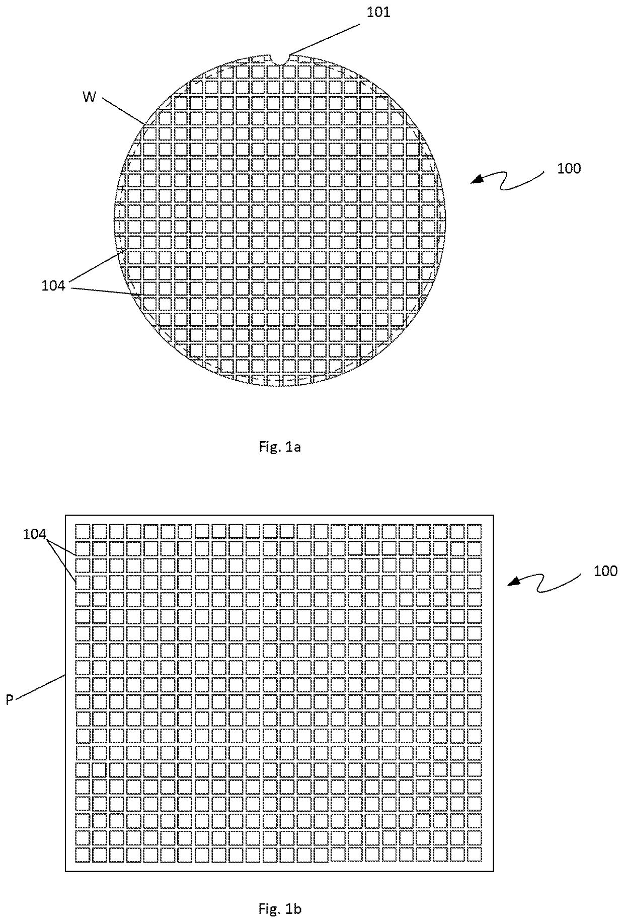
[0045]Lithographic processing to create semiconductor or other electronic devices is carried out on many different types of substrates 100. One of the most common is a semiconductor wafer W such as that shown in FIG. 1a. Wafer W is generally a flat discoid object of varying diameter. The wafer W generally includes an orientation structure 101 such as the illustrated notch. Marks, flats and other structures may be substituted for a notch. Wafers W are generally formed of a semiconductor material such as silicon, gallium arsenide, and the like, though in some instances glass or composite materials such as epoxy are used. These wafers W are commonly found in 200 mm or 300 mm diameters, but larger and smaller wafers W are common.

[0046]FIG. 1b illustrates a generic panel P of a type commonly addressed using lithographic processes. As with wafers W, panels P may be formed of semiconductor materials or of glass or composite materials. Panels P are generally rectangular or square in shape. ...


PUM

PropertyMeasurementUnit
diametersaaaaaaaaaa
diametersaaaaaaaaaa
poweraaaaaaaaaa

Abstract

A method for correcting misalignments is provided. An alignment for each device of a group of devices mounted on a substrate is determined. An alignment error for the group of devices mounted on the substrate is determined based on the respective alignment for each device. One or more correction factors are calculated based on the alignment error. The alignment error is corrected based on the one or more correction factors.

Description

CROSS-REFERENCE TO RELATED APPLICATIONS[0001]This application is a national stage under 35 U.S.C. § 371 of International Patent Application No. PCT / US2018 / 053254, filed Sep. 28, 2018, which claims the benefit of U.S. Provisional Application No. 62 / 565,940, filed Sep. 29, 2017, the disclosures of which are incorporated herein by reference in their entirety.INTRODUCTION[0002]The present invention relates generally to semiconductor devices and more particularly to a method for fabricating semiconductor devices.[0003]Semiconductor devices are an essential component of modern electronic and computing devices. Semiconductors devices are electronic components that exploit the electrical properties of semiconductor materials. The electrical conductivity of semiconductor materials can be manipulated by the introduction of an electric or magnetic field. Improvements in the manufacturing process have resulted in exponential improvements in the size, speed, and cost of semiconductor devices. Ho...

Claims


Application Information

Patent Timeline
Patent Type & Authority Patents(United States)
IPC IPC(8): G03F7/20G03F9/00
CPCG03F9/7023G03F7/70433G03F7/70516G03F7/70425G03F7/70491G03F9/7003
Inventor DA SILVEIRA, ELVINOBEST, KEITH FRANKFITZGERALD, WAYNELU, JIANSONG, XINDONAHER, J. CASEYMCLAUGHLIN, CHRISTOPHER J.
Owner ONTO INNOVATION INC
Why Eureka
Try Eureka