
Carbon metal interfaces for electrical connections, electronic and micro circuitry

Active Publication Date: 2021-03-02
BELLEZZA ANTHONY PAUL
View PDF5 Cites 0 Cited by
  • Summary
  • Abstract
  • Description
  • Claims
  • Application Information

AI Technical Summary

Benefits of technology

The present invention solves the problem of high electrical resistance and maintains the electrical performance of thermoelectric devices by impregnating graphene carbon molecules with the crystalline structure of the thermoelectric semiconductor. This results in a strong fusion layer that withstands stresses caused by mechanical bending and high temperature gradients. The invention also utilizes carbon structures as diffusion barriers and to protect against oxidation and contamination. The formation of fusion interfaces between the graphene carbon and a metal component requires the metal component to want carbon in its crystalline lattice. The resulting fusion layer dynamically adjusts its properties to the thermoelectric semiconductor and the metal conductor, providing a temperature and current tolerant superconducting interface.

Problems solved by technology

Electroplated and Electro-less nickels fail to protect the semiconductors from contamination due to micro-cracking in thermoelectric refrigeration devices and delamination in thermoelectric generators.
Solders fail to withstand high currents, melt under high temperatures, crack and delaminate under the mechanical stress of low temperatures, fail to support superconductivity and produce high electrical resistivity.

Method used


Image

  • Carbon metal interfaces for electrical connections, electronic and micro circuitry
  • Carbon metal interfaces for electrical connections, electronic and micro circuitry
  • Carbon metal interfaces for electrical connections, electronic and micro circuitry

Examples


Embodiment Construction

[0030]The terminology used herein is for the purpose of describing particular embodiments only and is not intended to be limiting of the invention. As used herein, the term “and / or” includes any and all combinations of one or more of the associated listed items. As used herein, the singular forms “a,”“an,” and “the” are intended to include the plural forms as well as the singular forms, unless the context clearly indicates otherwise. It will be further understood that the terms “comprises” and / or “comprising,” when used in this specification, specify the presence of stated features, steps, operations, elements, and / or components, but do not preclude the presence or addition of one or more other features, steps, operations, elements, components, and / or groups thereof.

[0031]Unless otherwise defined, all terms (including technical and scientific terms) used herein have the same meaning as commonly understood by one having ordinary skill in the art to which this invention belongs. It wi...


PUM


Abstract

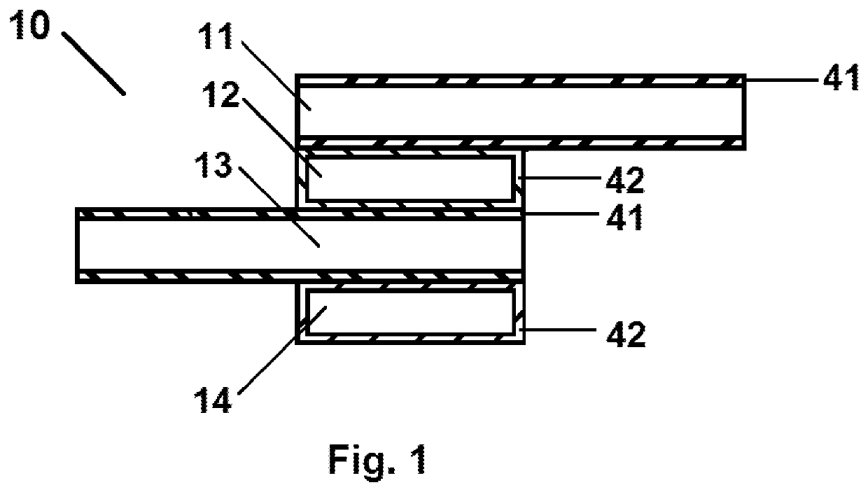
There are two parts to build fusion carbon metal interconnects. First are the fusing metals / alloys, typically in the Martensite phase and lacking carbon. Second are carbonized materials that have carbon infused. These carbonized materials may be referred to as carbon donating materials. Both parts can be interchanged as the substrate or mounted component, or the parts can form linear interface connections. The finished interfaces have very low electrical resistance and / or zero interface electrical resistance. The interconnect circuit topography materials and connections are endless and is dependent on circuit design. One example of such interface is a solderless thermoelectric device capable of use at higher operating temperatures as compared to conventional low temperature solders thus allowing the thermoelectric device to be used in a Seebeck device, for example. The thermoelectric device forms a fusion layer between a copper metal layer and a semiconductor wafer layer to create a true metallurgical bond.

Description

CROSS-REFERENCE TO RELATED APPLICATIONS[0001]This application is a continuation-in-part of U.S. patent application Ser. No. 16 / 154,594, filed Oct. 8, 2018, currently pending, which is a continuation of U.S. patent application Ser. No. 15 / 608,674, filed May 30, 2017, now U.S. Pat. No. 10,096,761, issued on Oct. 9, 2018.BACKGROUND OF THE INVENTION[0002]1. Field of the Invention[0003]One or more embodiments of the invention relates generally to carbon metal interfaces. More particularly, the invention relates to solderless thermoelectric interfaces that provide a true metallurgical bond of the device layers with superconducting interfaces and proper thermoelectric properties that are needed for electrical generation devices Seebeck devices) and cooling devices (Peltier devices), for example.[0004]2. Description of Prior Art and Related Information[0005]The following background information may present examples of specific aspects of the prior art (e.g., without limitation, approaches, f...

Claims


Application Information

Patent Timeline
IPC IPC(8): H01L35/32H01L35/08H01L35/34H01L35/16
CPCH01L35/32H01L35/08H01L35/16H01L35/325H01L35/34H10N10/817H10N10/852H10N10/01H10N10/17H10N19/101
Inventor BELLEZZA, ANTHONY PAUL
Owner BELLEZZA ANTHONY PAUL
Learn More