Thin-film transistor array substrate and manufacturing method for the same

a technology of thin film transistors and manufacturing methods, applied in the field of display technology, can solve the problems of high cost and complex process, and achieve the effects of reducing process, saving cost, and facilitating breakag

Active Publication Date: 2020-02-04
SHENZHEN CHINA STAR OPTOELECTRONICS SEMICON DISPLAY TECH CO LTD
View PDF9 Cites 0 Cited by
  • Summary
  • Abstract
  • Description
  • Claims
  • Application Information

AI Technical Summary

Benefits of technology

[0005]The technology problem solved by the embodiment of the present invention is to provide a thin-film transistor array substrate and a manufacturing method for the same such that the number of masks required for manufacturing the thin-film transistor array substrate is reduced.
[0015]The embodiment of the present invention has following beneficial effect: because the gate insulation layer is directly deposited, the gate insulation layer covers the gate electrode and the first storage electrode without using a mask to patterning the gate insulation layer. Accordingly, comparing to the conventional art, the number of the masks for manufacturing the thin-film transistor substrate is reduce from seven to six such that one mask is saved, cost is saved and process is reduced. Besides, in the present embodiment, because the storage capacitor includes at least a portion of the gate insulation layer, the gate insulation layer is denser so that the storage capacitor is not easily to be broken through.

Problems solved by technology

Accordingly, the entire thin-film transistor array substrate requires 7 masks such that the number of the mask is higher, the cost is higher and the process is complex.

Method used


Image

  • Thin-film transistor array substrate and manufacturing method for the same
  • Thin-film transistor array substrate and manufacturing method for the same
  • Thin-film transistor array substrate and manufacturing method for the same

Examples


Embodiment Construction

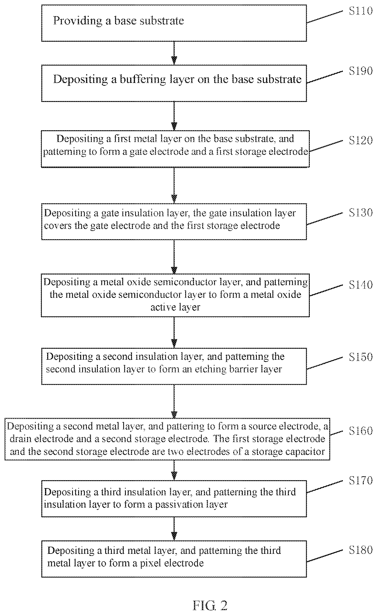
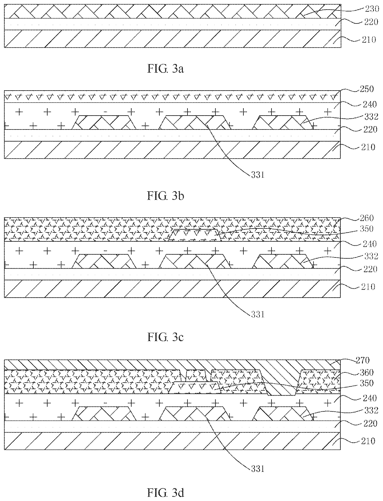
[0021]The following content combines with the drawings and the embodiment for describing the present invention in detail. It is obvious that the following embodiments are only some embodiments of the present invention. For the person of ordinary skill in the art without creative effort, the other embodiments obtained thereby are still covered by the present invention.

[0022]Moreover, the terms “comprise,” include,” or any other variation thereof, are intended to cover a non-exclusive inclusion, such that a series of elements including the process, method, article or device that includes not only those elements but also other elements not expressly listed or further comprising such process, method, article or device inherent elements. Without more constraints, by the statement “comprises one . . . ” element defined does not exclude the existence of additional identical elements in the process, method, article, or apparatus. In the specification, claims, and accompanying drawings of th...


PUM

PropertyMeasurementUnit
temperatureaaaaaaaaaa

Abstract

A manufacturing method for a thin-film transistor array substrate is disclosed. The method includes: providing a base substrate; depositing a first metal layer on the base substrate, and patterning to form a gate electrode and a first storage electrode; depositing a gate insulation layer, wherein the gate insulation layer covers the gate electrode and the first storage electrode; depositing a metal oxide semiconductor layer, and patterning to form a metal oxide active layer; depositing a second insulation layer, and patterning to form an etching barrier layer; depositing a second metal layer, and pattering to form a source electrode, a drain electrode and a second storage electrode, wherein the first storage electrode and the second storage electrode are two electrodes of a storage capacitor; depositing a third insulation layer, and patterning to form a passivation layer; and depositing a third metal layer, and patterning to form a pixel electrode.

Description

CROSS REFERENCE[0001]This application is a continuing application of PCT Patent Application No. PCT / CN2018 / 078339, entitled “THIN-FILM TRANSISTOR ARRAY SUBSTRATE AND MANUFACTURING METHOD FOR THE SAME”, filed on Mar. 7, 2018, which claims priority to China Patent Application No. CN 201810111246.4 filed on Feb. 5, 2018, both of which are hereby incorporated in its entireties by reference.FIELD OF THE INVENTION[0002]The present invention relates to a display technology field, and more particularly to a thin-film transistor array substrate and a manufacturing method for the same.BACKGROUND OF THE INVENTION[0003]In a conventional thin-film transistor array substrate, with reference to FIG. 1, the thin-film transistor array substrate includes: a base substrate 110, a buffering layer 120, a gate electrode 131, a first storage electrode 132, a gate insulation layer 140, a metal oxide active layer 150, an etching barrier layer 160, a source electrode 171, a drain electrode 172, a second stor...

Claims


Application Information

Patent Timeline
Patent Type & Authority Patents(United States)
IPC IPC(8): H01L27/12H01L29/66H01L29/786
CPCH01L29/7869H01L29/66969H01L27/127H01L27/1255H01L27/1225
Inventor ZHOU, XINGYU
Owner SHENZHEN CHINA STAR OPTOELECTRONICS SEMICON DISPLAY TECH CO LTD
Why Eureka
Try Eureka