Methods of forming inverted multijunction solar cells with distributed Bragg reflector
a solar cell and bragg reflector technology, applied in the direction of sustainable manufacturing/processing, climate sustainability, semiconductor devices, etc., can solve the problems of increasing manufacturing complexity, presenting a number of practical difficulties, and the materials and fabrication steps disclosed in the prior art have not been adequate to produce a commercially viable and energy efficient inverted metamorphic multijunction solar cell using commercially established fabrication processes. , to achieve the effect of reducing the diffusion length necessary, increasing the radiation hardness of the solar
- Summary
- Abstract
- Description
- Claims
- Application Information
AI Technical Summary
Benefits of technology
Problems solved by technology
Method used
Image
Examples
second embodiment
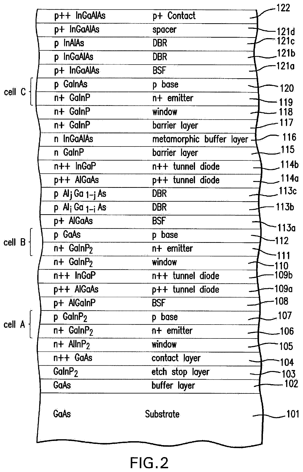
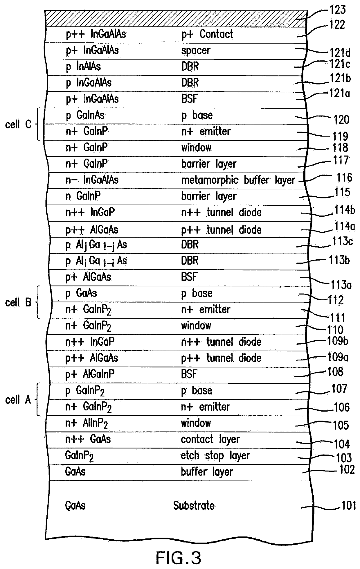
[0097]Although one embodiment of the present invention utilizes a plurality of layers of InGaAlAs for the metamorphic layer 116 for reasons of manufacturability and radiation transparency, other embodiments of the present invention may utilize different material systems to achieve a change in lattice constant from subcell B to subcell C. Thus, the system of Wanlass using compositionally graded InGaP is the present invention. Other embodiments of the present invention may utilize continuously graded, as opposed to step graded, materials. More generally, the graded interlayer may be composed of any of the As, N, Sb based III-V compound semiconductors subject to the constraints of having the in-plane lattice parameter greater or equal to that of the second solar cell and less than or equal to that of the third solar cell, and having a band gap energy greater than that of the second solar cell.
[0098]In another embodiment of the present invention, an optional second barrier layer 117 may...
third embodiment
[0127]FIG. 14C is a cross-sectional view of the solar cell of FIG. 12B after the next process step in the present invention in which a cover glass 514 is secured to the top of the cell by an adhesive 513. The cover glass 514 is typically about 4 mils thick and preferably covers the entire channel 510, but does not extend to channel 511. Although the use of a cover glass is desirable for many environmental conditions and applications, it is not necessary for all implementations, and additional layers or structures may also be utilized for providing additional support or environmental protection to the solar cell.
[0128]FIG. 15 is a cross-sectional view of the solar cell of FIG. 14C after the next process step in some embodiments of the present invention in which the adhesive layer 124, the surrogate substrate 125 and the peripheral portion 512 of the wafer is entirely removed, leaving only the solar cell with the cover glass 514 (or other layers or structures) on the top, and the meta...
PUM
| Property | Measurement | Unit |
|---|---|---|
| band gap | aaaaa | aaaaa |
| band gap | aaaaa | aaaaa |
| band gaps | aaaaa | aaaaa |
Abstract
Description
Claims
Application Information
 - R&D
- Intellectual Property
- Life Sciences
- Materials
- Tech Scout
- Unparalleled Data Quality
- Higher Quality Content
- 60% Fewer Hallucinations
Browse by: Latest US Patents, China's latest patents, Technical Efficacy Thesaurus, Application Domain, Technology Topic, Popular Technical Reports.
© 2025 PatSnap. All rights reserved.Legal|Privacy policy|Modern Slavery Act Transparency Statement|Sitemap|About US| Contact US: help@patsnap.com


