Method for rewriting semiconductor storage device and the semiconductor storage device
a semiconductor storage device and a technology for rewriting semiconductors, applied in information storage, static storage, digital storage, etc., can solve the problems of affecting the timing of applying the write voltage, affecting the stability of the mos transistor, so as to reduce the occurrence of a plurality of unstable waveform application pulses and the variation of the width of the application pulses
- Summary
- Abstract
- Description
- Claims
- Application Information
AI Technical Summary
Benefits of technology
Problems solved by technology
Method used
Image
Examples
embodiment 1
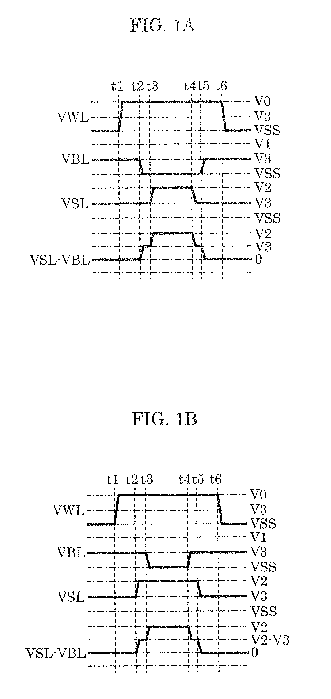
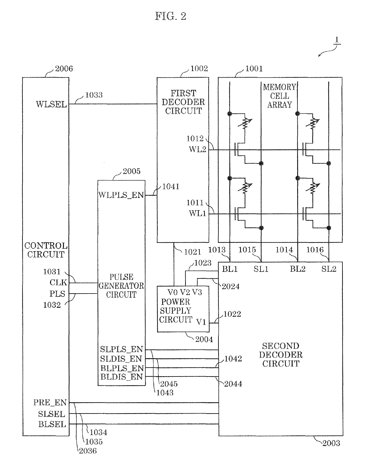
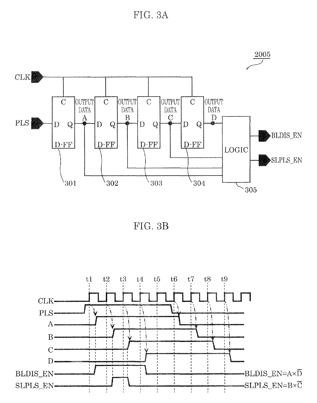
[0105]Hereinafter, Embodiment 1 is described with reference to FIG. 1A to FIG. 4C.
[0106]FIGS. 1A and 1B are each a timing chart of rewriting semiconductor storage device 1 according to Embodiment 1.
[0107]FIGS. 1A and 1B are each indicates a bias state at the time when a selected memory cell is set to LR.
[0108]Here, at least one word line is selected from among the plurality of word lines as a selected word line. In addition, at least one bit line is selected from among the plurality of bit lines as a selected bit line, and at least one source line is selected from among the plurality of source lines as a selected source line.
[0109]First, pre-charge voltage V3 is applied to both of the plurality of bit lines and the plurality of source lines (a first rewriting step). Next, a rewrite voltage (VSS (=0 V), V1 or V2) is applied to one of the selected bit line or the selected source line (a second rewriting step). Next, a rewrite voltage (VSS (=0 V), V1 or V2) is applied to both of the se...
embodiment 2
[0138]Hereinafter, Embodiment 2 is described with reference to FIG. 5A to FIG. 5E.
[0139]The configuration of semiconductor storage device 2 according to this embodiment is the same as that of semiconductor storage device 1, and thus descriptions thereof are not repeated.
[0140]FIGS. 5A to 5E are each a timing chart of rewriting semiconductor storage device 2 according to Embodiment 2.
[0141]FIGS. 5A to 5E each illustrate a bias state at the time when a selected memory cell is set to LR.
[0142]Here, at least one word line is selected from among the plurality of word lines as a selected word line. In addition, at least one bit line is selected from among the plurality of bit lines as a selected bit line, and at least one source line is selected from among the plurality of source lines as a selected source line.
[0143]First, pre-charge voltage V3 is applied to both of the plurality of bit lines and the plurality of source lines (a first rewriting step). Next, both of the selected bit line ...
embodiment 3
[0151]Hereinafter, Embodiment 3 is described with reference to FIG. 6.
[0152]The configuration of semiconductor storage device 3 according to this embodiment is the same as that of semiconductor storage device 1, and thus descriptions thereof are not repeated.
[0153]FIG. 6 is a timing chart of rewriting semiconductor storage device 3 according to Embodiment 3.
[0154]FIG. 6 indicates a bias state at the time when a selected memory cell is set to LR.
[0155]Here, at least one word line is selected from among the plurality of word lines as a selected word line. In addition, at least one bit line is selected from among the plurality of bit lines as a selected bit line, and at least one source line is selected from among the plurality of source lines as a selected source line.
[0156]First, pre-charge voltage V3 is applied to both of the plurality of bit lines and the plurality of source lines (a first rewriting step). Next, both of the selected bit line and the selected source line are grounde...
PUM
 Abstract
Description
Claims
Application Information
 - R&D
- Intellectual Property
- Life Sciences
- Materials
- Tech Scout
- Unparalleled Data Quality
- Higher Quality Content
- 60% Fewer Hallucinations
Browse by: Latest US Patents, China's latest patents, Technical Efficacy Thesaurus, Application Domain, Technology Topic, Popular Technical Reports.
© 2025 PatSnap. All rights reserved.Legal|Privacy policy|Modern Slavery Act Transparency Statement|Sitemap|About US| Contact US: help@patsnap.com


