
Apparatus and method for contactless transfer and soldering of chips using a flash lamp

a technology of flash lamps and apparatus, applied in electrical apparatus, semiconductor devices, semiconductor/solid-state device details, etc., can solve the problems of reflow soldering, low decomposition temperature of polyester foils, time-consuming process using large in-line ovens, etc., to achieve high temperature, prevent overheating, and relatively fast heating

Active Publication Date: 2019-05-28
NEDERLANDSE ORG VOOR TOEGEPAST-NATUURWETENSCHAPPELIJK ONDERZOEK (TNO)
View PDF7 Cites 0 Cited by
  • Summary
  • Abstract
  • Description
  • Claims
  • Application Information

AI Technical Summary

Benefits of technology

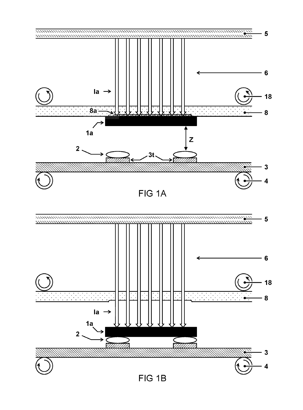
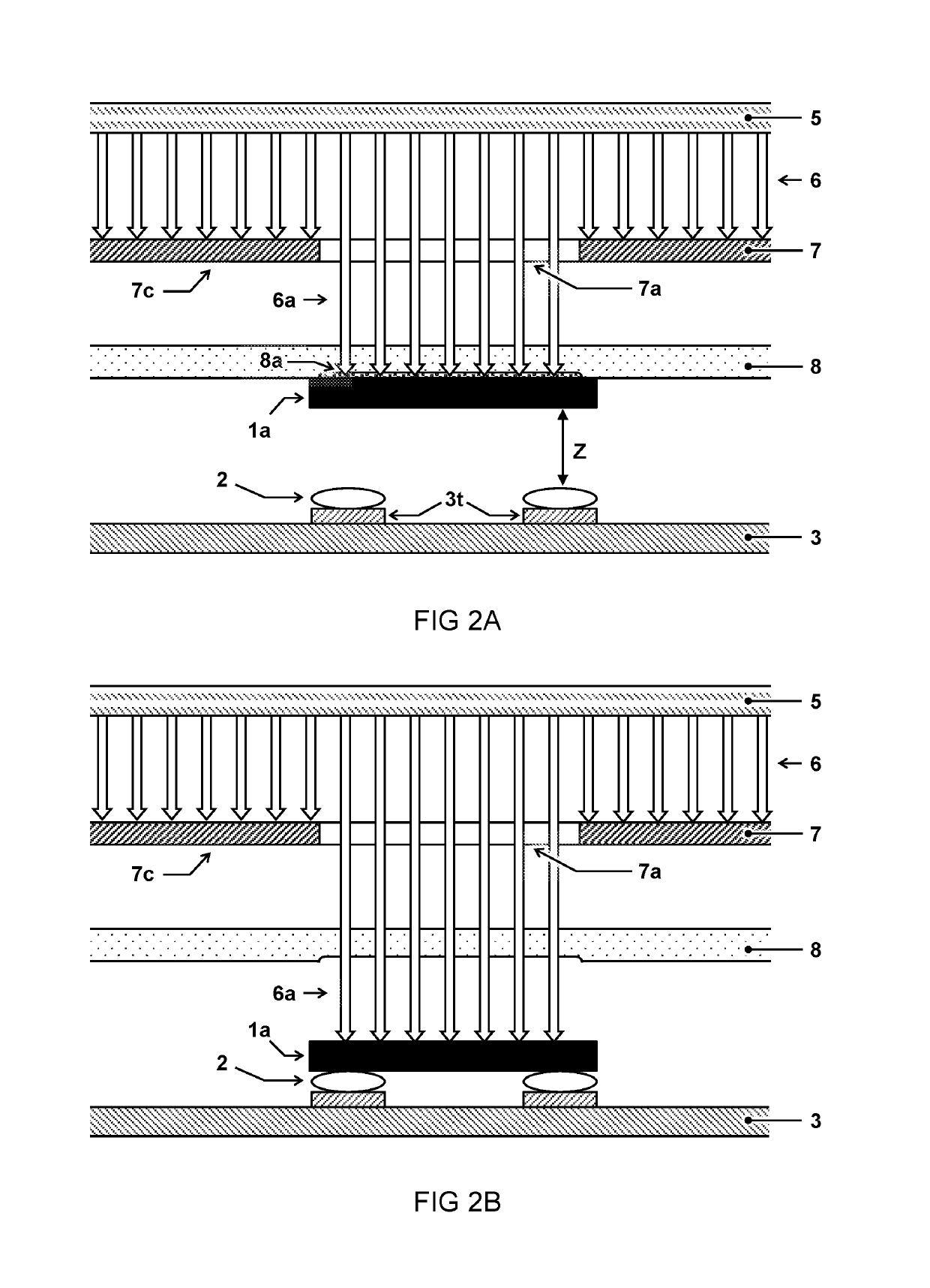
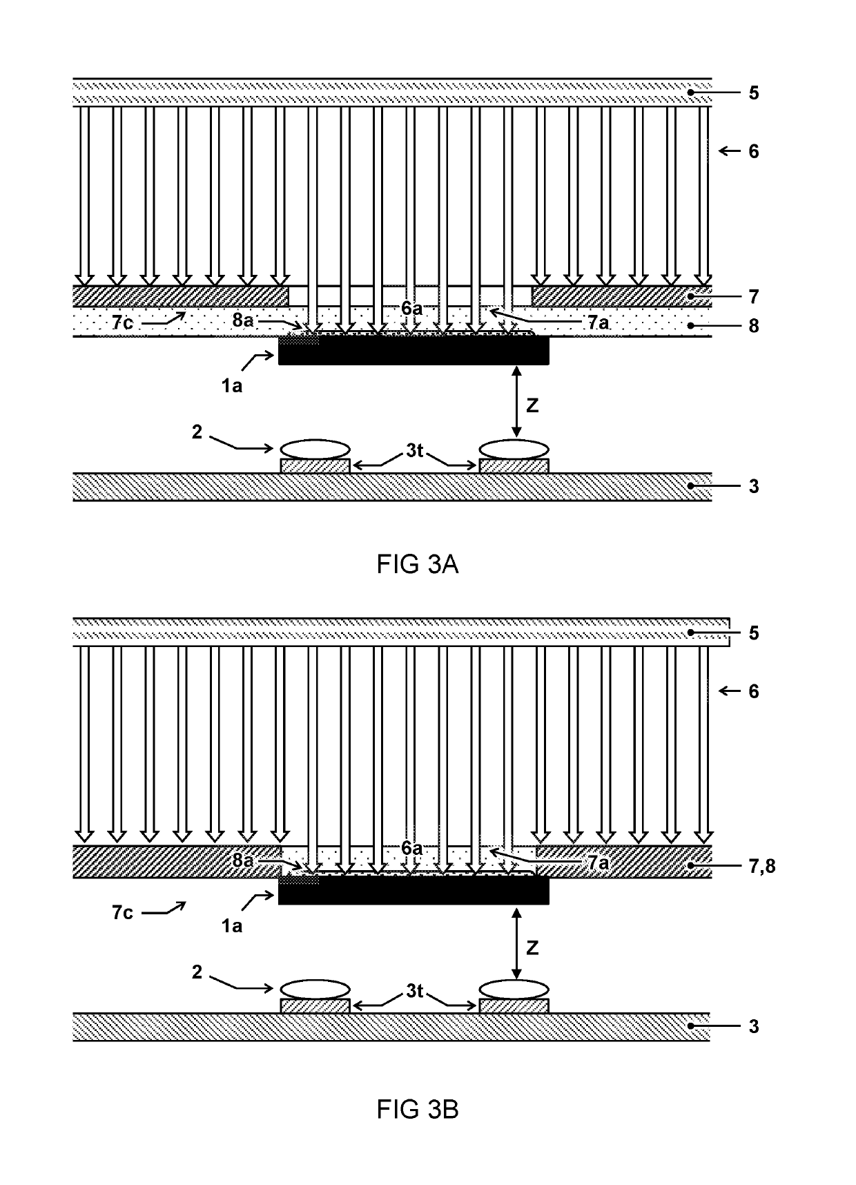
The patent describes a method and apparatus for heating and transferring electronic chips using a light pulse from a flash lamp. The light pulse can be used to release the chips from their carrier substrate and heat them for soldering. The use of a masking device with different light intensities can compensate for different heating properties of the chips, resulting in controlled and uniform heating and soldering. The method can be used for simultaneous transfer of multiple chips and can be controlled to prevent damage to the substrate. The apparatus includes a masking device and a chip carrier foil for contactless transfer of chips from the carrier to the destination substrate.

Problems solved by technology

However, for more complex systems, there is a need to develop hybrid systems in which printed circuitry is combined with silicon-based integrated circuits or surface mounted device (SMD) components, referred herein as chip components or simply “chips”.
However, these processes are considered time consuming and / or incompatible with low-cost polyester foils having low decomposition temperatures.
However, reflow soldering, is poorly compatible with low-cost flexible foils and roll-to-roll (R2R) processing because it requires maintaining the whole board above the liquidus temperature of the solder which is generally above 200° C. for long holding time.
This typically results in a time-consuming process using large in-line ovens, often having multiple loops.
The long holding time may also cause deformation or degradation of the flexible foil itself or degradation of its organic surface coatings or adhesives.
However, in laser spot soldering, the small spot area may require precise positioning of the spot for each component.
Furthermore, applying this technology in a R2R process is challenging as the laser spot needs to align to multiple chips on a moving substrate.
Furthermore, the process can be time consuming.
However, if the absorption of light by the (foil) substrate and / or components differs, this can lead to selective heating.
This may lead to further differences in heating behaviour for the different components which makes the temperature and solder process difficult to control.
Furthermore, decomposition by heating may cause rapid gas formation that can increase impulse of the chip thereby launching it towards the substrate.
The different heating properties can make it difficult to uniformly control the transfer and soldering.

Method used


Image

  • Apparatus and method for contactless transfer and soldering of chips using a flash lamp
  • Apparatus and method for contactless transfer and soldering of chips using a flash lamp
  • Apparatus and method for contactless transfer and soldering of chips using a flash lamp

Examples


Embodiment Construction

[0031]In some instances, detailed descriptions of well-known devices and methods may be omitted so as not to obscure the description of the present systems and methods. Terminology used for describing particular embodiments is not intended to be limiting of the invention. As used herein, the singular forms “a”, “an” and “the” are intended to include the plural forms as well, unless the context clearly indicates otherwise. The term “and / or” includes any and all combinations of one or more of the associated listed items. It will be understood that the terms “comprises” and / or “comprising” specify the presence of stated features but do not preclude the presence or addition of one or more other features. It will be further understood that when a particular step of a method is referred to as subsequent to another step, it can directly follow said other step or one or more intermediate steps may be carried out before carrying out the particular step, unless specified otherwise. Likewise i...


PUM


Abstract

A method and apparatus for soldering a chip (1a) to a substrate (3). A chip carrier (8) is provided between a flash lamp (5) and the substrate (3). The chip (1a) is attached to the chip carrier (8) on a side of the chip carrier (8) facing the substrate (3). A solder material (2) is disposed between the chip (1a) and the substrate (3). The flash lamp (5) generates a light pulse (6) for heating the chip (1a). The heating of the chip (1a) causes the chip (1a) to be released from the chip carrier (8) towards the substrate (3). The solder material (2) is at least partially melted by contact with the heated chip (1a) for attaching the chip (1a) to the substrate (3).

Description

CROSS-REFERENCE TO RELATED APPLICATIONS[0001]This patent application is a U.S. National Phase of PCT International Application No. PCT / NL2016 / 050296, filed Apr. 26, 2016, which claims priority to European Application No. 15165474.6, filed Apr. 28, 2015, which are both expressly incorporated by reference in their entireties, including any references contained therein.TECHNICAL FIELD AND BACKGROUND[0002]The present disclosure relates to soldering, in particular to an apparatus and method for soldering chips to a substrate.[0003]Simple flexible systems, such as logic functions with transistors or optoelectronic devices, can in principle be fully printed on a substrate (e.g. foil or rigid board). However, for more complex systems, there is a need to develop hybrid systems in which printed circuitry is combined with silicon-based integrated circuits or surface mounted device (SMD) components, referred herein as chip components or simply “chips”. To functionalize the device, multiple chip...

Claims


Application Information

Patent Timeline
Patent Type & Authority Patents(United States)
IPC IPC(8): H01L21/673H01L21/683H01L21/677H01L21/60H01L23/00
CPCH01L21/67356H01L21/67751H01L21/683H01L21/6835H01L21/6836H01L24/75H01L24/81H01L24/97H01L2224/97H01L2224/81815H01L2224/81224H01L2224/81193H01L2224/81192H01L2224/81191H01L2224/8123H01L2224/81005H01L2224/75824H01L24/11H01L24/13H01L24/16H01L2021/60007H01L2221/68354H01L2221/68381H01L2224/1131H01L2224/1132H01L2224/131H01L2224/16227H01L2224/759H01L2224/7526H01L2224/7565H01L2224/7598H01L2224/75252H01L2224/75253H01L2224/75502H01L2224/75611H01L2224/75702H01L2224/75753H01L2224/75804H01L2924/014H01L2224/81H01L2924/00012H01L2924/00014H01L2224/95001
Inventor HENDRIKS, ROB JACOBVAN DEN ENDE, DAAN ANTONSMITS, EDSGER CONSTANT PIETER
Owner NEDERLANDSE ORG VOOR TOEGEPAST-NATUURWETENSCHAPPELIJK ONDERZOEK (TNO)
Learn More