Substrate defect inspection apparatus, method of adjusting sensitivity parameter value for substrate defect inspection, and non-transitory storage medium

a substrate defect and inspection method technology, applied in semiconductor/solid-state device testing/measurement, image enhancement, instruments, etc., can solve the problems of insufficient prevention of false defects, insufficient solution, and high labor and time, so as to ease eliminate the burden on the operator who performs the adjustment of the sensitivity parameter value by trial and error, and ensure the effect of stability

Active Publication Date: 2019-04-02
TOKYO ELECTRON LTD
View PDF3 Cites 0 Cited by
  • Summary
  • Abstract
  • Description
  • Claims
  • Application Information

AI Technical Summary

Benefits of technology

[0007]The present invention has been made to solve the problem, and its object is to enable automatic adjustment of a parameter value used at the time of defect inspection on a substrate, and decrease the detection frequency of a false defect at the time of the defect inspection on a substrate.
[0026]The present invention compares the image data obtained by picking up an image of the entire front surface of the substrate and the reference pixel data and automatically adjusts the sensitivity parameter value for determining whether or not the substrate is defective. More specifically, the present invention selects a plurality of virtual inspection substrates from among a plurality of substrates inspected earlier than the adjustment time of the sensitivity parameter value, performs virtual inspection by comparing new reference pixel data after the adjustment of the sensitivity parameter and the image data, and eases the sensitivity parameter value so as to prevent, when a certain substrate is determined to be a false defective substrate, the substrate from being determined to be a defective substrate in actual inspection.
[0027]The present invention further performs, in sequence on the plurality of selected virtual inspection substrates, the above operations, namely, selecting a plurality of virtual inspection substrates from among a plurality of substrates inspected earlier than the adjustment time of the sensitivity parameter value, performing virtual inspection by comparing new reference pixel data after the adjustment of the sensitivity parameter and the image data, and easing the sensitivity parameter value as described above, and uses a finally acquired sensitivity parameter value as a new sensitivity parameter value. Accordingly, the burden on the operator who performs the adjustment of the sensitivity parameter value by trial and error is eliminated, and stable substrate defect inspection can also be realized.

Problems solved by technology

However, as for the above parameter, many parameters exist, and therefore the operator of an apparatus comes to repeat operations of changing the parameters and checking the influence of the change on the inspection many times, requiring a lot of labor and time as a result of the trial and error.
In other words, the accuracy of the inspection is influenced by the level of skill of the operator setting the parameter values, thus possibly failing to sufficiently prevent the false defect.
In this regard, Japanese Patent Application Publication No. 2014-115140 discloses a method of creating reference image data, but does not describe a method of setting the above parameter value, which is insufficient to solve this problem.

Method used


Image

  • Substrate defect inspection apparatus, method of adjusting sensitivity parameter value for substrate defect inspection, and non-transitory storage medium
  • Substrate defect inspection apparatus, method of adjusting sensitivity parameter value for substrate defect inspection, and non-transitory storage medium
  • Substrate defect inspection apparatus, method of adjusting sensitivity parameter value for substrate defect inspection, and non-transitory storage medium

Examples


Embodiment Construction

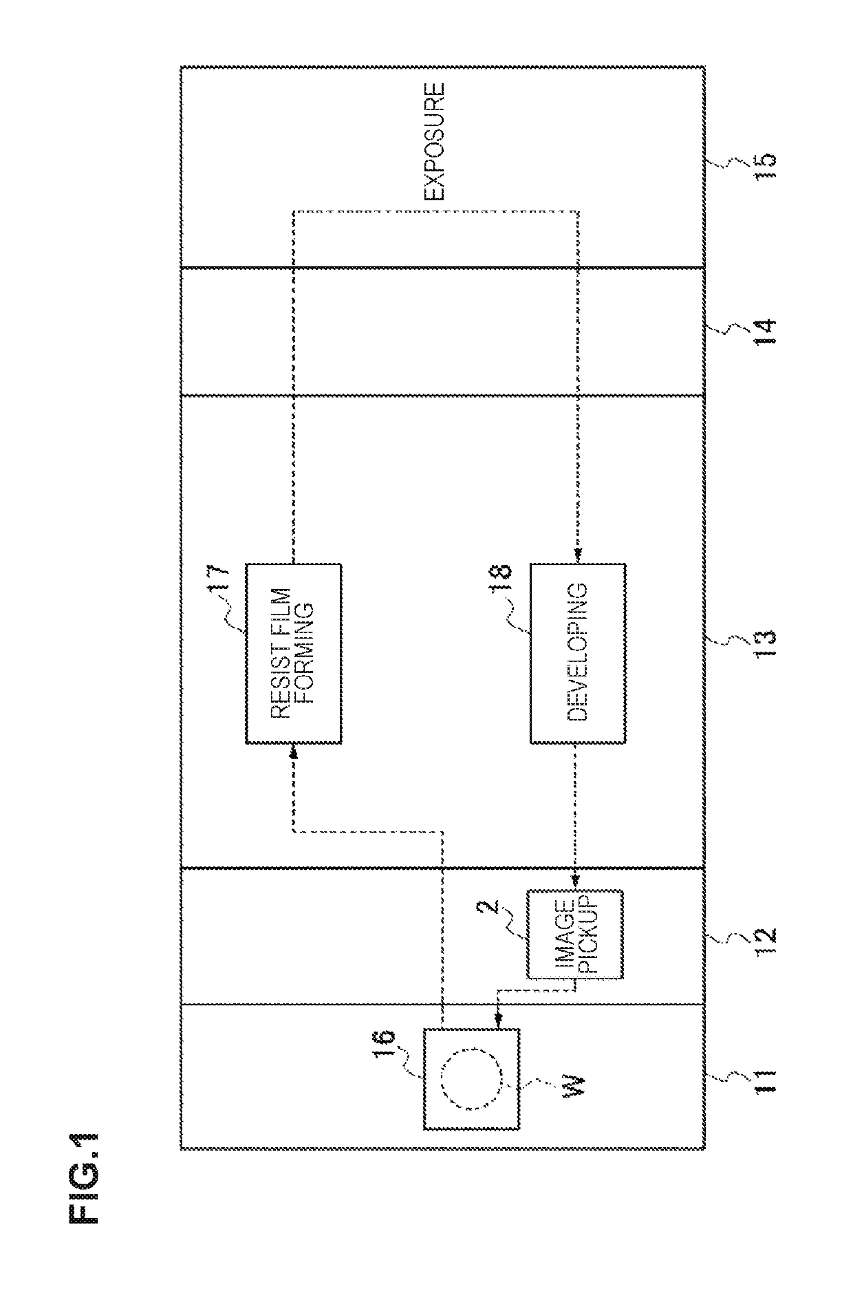
[0041]A coating and developing apparatus 1 being one embodiment to which the present invention is applied will be explained referring to a schematic plan view in FIG. 1. The coating and developing apparatus 1 is composed of a carrier block 11, an intermediate block 12, a treatment block 13, and an interface block 14 which are connected in this order in a linear arrangement in a horizontal direction. To the interface block 14, an exposure apparatus 15 is connected. A carrier 16 in which wafers W being substrates are stored is transferred to and mounted on the carrier block 11 by a not-illustrated transfer mechanism. In the treatment block 13, a resist film forming module 17 that supplies a resist solution to the front surface of the wafer W to form a resist film, and a developing module 18 that supplies a developing solution to the resist film exposed along a predetermined pattern in the exposure apparatus 15 to form a resist pattern, are provided. In the intermediate block 12, an im...


PUM

PropertyMeasurementUnit
defect inspectionaaaaaaaaaa
defectaaaaaaaaaa
brightnessaaaaaaaaaa

Abstract

A method of adjusting a sensitivity parameter value for substrate defect inspection used in a substrate defect inspection apparatus compares, for each pixel value of a selected virtual inspection substrate, using reference pixel data to be used after adjustment, the deviation amount from an allowable range corresponding to the position thereof and the sensitivity parameter value before the adjustment when each pixel value is deviated from the allowable range, and updates the deviation amount as a new sensitivity parameter value when the deviation amount exceeds the sensitivity parameter value and a difference between the deviation amount and the sensitivity parameter value is equal to or less than a threshold value.

Description

CROSS REFERENCE TO RELATED APPLICATION[0001]This application is based upon and claims the benefit of priority of the prior Japanese Patent Application No. 2016-130593, filed in Japan on Jun. 30, 2016, the entire contents of which are incorporated herein by reference.BACKGROUND OF THE INVENTION1. Field of the Invention[0002]The present invention relates to a defect inspection apparatus for determining a defect of a substrate using image data obtained by picking up an image of the substrate, a method of adjusting a sensitivity parameter value for substrate defect inspection, and a non-transitory storage medium storing a computer program used for the defect inspection apparatus.2. Description of the Related Art[0003]In a photolithography process being one of manufacturing processes of a semiconductor device, formation of a resist film by applying a resist onto the front surface of a semiconductor wafer (hereinafter, described as a wafer) being a substrate, and exposure and development ...

Claims


Application Information

Patent Timeline
Patent Type & Authority Patents(United States)
IPC IPC(8): G06K9/00G06T7/00G06T7/90G01N21/95
CPCG06T7/90G06T7/0008G01N21/9501G01N2201/12G06T2207/30148G03F7/7065G06T7/001H01L22/12H01L22/30H01L22/24G01N21/95607
Inventor KITADA, YASUHIROHASEGAWA, IZUMITOMITA, HIROSHINAKAYAMA, KOUSUKENISHIYAMA, TADASHI
Owner TOKYO ELECTRON LTD
Why Eureka
Try Eureka