Semiconductor device
A semiconductor and remote control device technology, which is applied in semiconductor devices, semiconductor/solid-state device manufacturing, transistors, etc., can solve problems such as uneven crystal grain size, achieve excellent characteristics, high yield, and reduce characteristic changes.
- Summary
- Abstract
- Description
- Claims
- Application Information
AI Technical Summary
Problems solved by technology
Method used
Image


Examples
Embodiment approach 1
[0042] A state in which a CW laser beam is scanned on the surface of a semiconductor film formed on a substrate and a manufactured TFT will be described with reference to FIGS. 1A to 1C.
[0043] FIG. 1A is a plan view showing a scanning state of a laser beam 11 on the surface of an amorphous semiconductor film. A laser beam 11 has an elongated elliptical beam spot and is scanned in a scanning direction 12 indicated by an arrow in the figure to partially form a crystal region.
[0044] Although not shown in FIG. 1A, since the figure shows an example of forming a top gate type TFT, a base insulating film is formed over a substrate having an insulating surface and an amorphous semiconductor film is formed thereon.
[0045] In the crystallization process of an amorphous semiconductor film, a continuous wave solid-state laser is used in this embodiment mode and a laser beam having the second, third, or fourth harmonic of the fundamental wave is emitted onto the semiconductor film ...
Embodiment approach 2
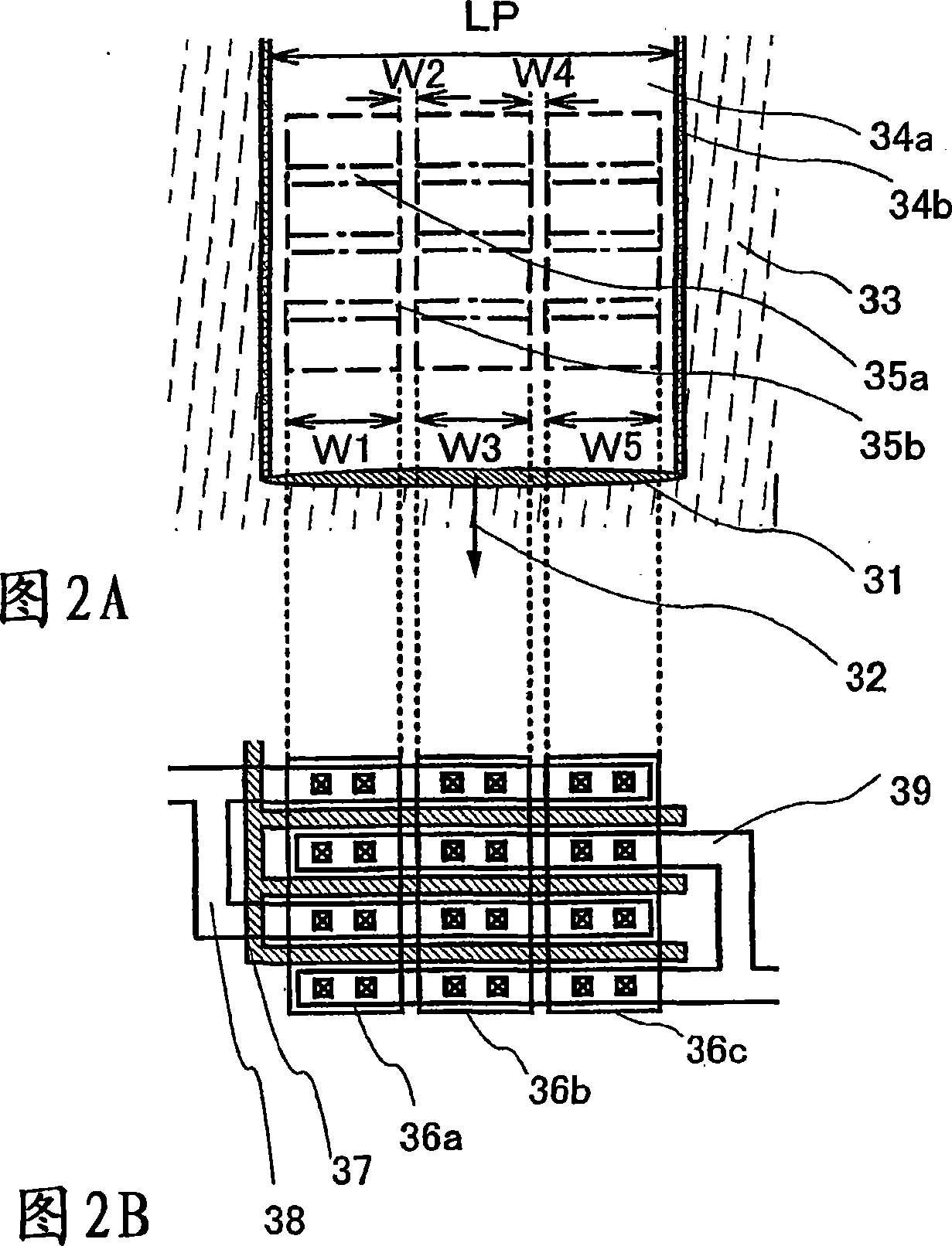
[0068] A state in which a quasi-CW laser beam is scanned on the surface of a semiconductor film formed over a substrate and a manufactured TFT are described with reference to FIGS. 2A and 2B.
[0069] FIG. 2A is a plan view showing a scanning state of a laser beam 31 on the surface of an amorphous semiconductor film. A laser beam 31 has an elongated elliptical beam spot and is scanned in a scanning direction 32 indicated by an arrow in the figure to partially form a crystal region.
[0070] Although not shown in FIG. 2A, since the figure shows an example of forming a top gate type TFT, a base insulating film is formed on a substrate having an insulating surface and an amorphous semiconductor film is formed thereon.
[0071] In the process of crystallizing the amorphous semiconductor film, YVO with an output of 1.8W was used 4 laser with a repetition rate of 80 MHz and a pulse width of approximately 12 ps. The pulse repetition rate is not limited to 80 MHz in the present inve...
Embodiment 1
[0088] In Embodiment Mode 1, the configuration of the laser irradiation equipment will be described with reference to FIG. 3 .
PUM
 Abstract
Description
Claims
Application Information
 - R&D
- Intellectual Property
- Life Sciences
- Materials
- Tech Scout
- Unparalleled Data Quality
- Higher Quality Content
- 60% Fewer Hallucinations
Browse by: Latest US Patents, China's latest patents, Technical Efficacy Thesaurus, Application Domain, Technology Topic, Popular Technical Reports.
© 2025 PatSnap. All rights reserved.Legal|Privacy policy|Modern Slavery Act Transparency Statement|Sitemap|About US| Contact US: help@patsnap.com