Semiconductor storage device
A storage device and semiconductor technology, applied in information storage, static memory, digital memory information, etc., can solve the problems of complex structure of power supply system, no consideration of data stability, and inability to flexibly deal with discrete transistors of memory cells, etc. The effect of suppressing the increase in the layout area and simplifying the power supply structure
- Summary
- Abstract
- Description
- Claims
- Application Information
AI Technical Summary
Problems solved by technology
Method used
Image


Examples
no. 1 example
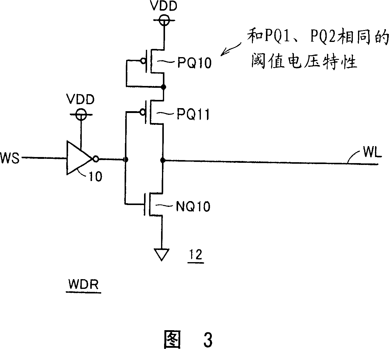
[0156] Fig. 13 is a diagram showing a modified example of the pull-down element according to the second embodiment of the present invention. In the structure shown in FIG. 13, pull-down element PD is constituted by N-channel MOS transistor NQ21 whose gate receives power supply voltage VDD. The drain of this MOS transistor NQ21 is connected to the word line WL, and the source is coupled to the ground node. The word line WL is driven by a word line driver WDV. The word line driver WDV has the same structure as that shown in FIG. 8 .
[0157] In the case of the pull-down element PD shown in FIG. 13 , the gate of the MOS transistor NQ21 receives the power supply voltage VDD, and is normally maintained in an on state to pull down the potential of the word line WL through its channel resistance. Therefore, when the word line is driven to the selected state, the MOS transistor NQ21 is turned on before the potential of the word line WL rises to equal to or higher than the threshold ...
no. 2 example
[0160] 14 is a diagram schematically showing the configuration of a second modified example of the semiconductor memory device according to the second embodiment of the present invention. FIG. 14 shows a case where pull-down element PDa is arranged close to word line driver WDV on word line WL, and pull-down element PDb is arranged far from word line driver WDV from word line WL. Either one of the pull-down elements Pda and PDb is used.
[0161] When the pull-down element PDa is arranged close to the word line driver WDV, the voltage level of the word line WL is set to the voltage level of VDD·Rn / (Rp+Rn) regardless of the wiring resistance Rw1 of the word line. Therefore, the potential of the word line WL can be set according to the value of the on-resistance Rn of the pull-down element PDa.
[0162] On the other hand, when pull-down element PDb is used, assuming that its on-resistance is Rn, voltage VWL1 of word line WL at the end near word line driver WDV is expressed by th...
no. 3 example
[0170] Fig. 15 is a diagram showing the structure of a third modified example of the second embodiment of the present invention. In FIG. 15, a pull-down element PD and a memory cell MC are shown. Pull-down element PD includes a plurality of parallel-connected unit N-channel MOS transistors NU0-NUk. The gates of these N-channel MOS transistors NU0-NUk are connected to the word line WL or commonly receive the power supply voltage VDD. These unit N-channel MOS transistors NU0-NUk have the same threshold voltage conditions as the drive transistors NQ1 and NQ2 of the memory cell MC. That is, the impurity implantation conditions, layout, and dimensions (ratio of channel width W to channel length, W / L) in the channel region are as close as possible to the drive of these unit N-channel MOS transistors NU0-Nuk and memory cells. Transistors NQ1-NQ2 are set identically. Therefore, these drive transistors NQ1 and NQ2 and unit N-channel MOS transistors NU0-NUk are formed by the same man...
PUM
 Abstract
Description
Claims
Application Information
 - R&D
- Intellectual Property
- Life Sciences
- Materials
- Tech Scout
- Unparalleled Data Quality
- Higher Quality Content
- 60% Fewer Hallucinations
Browse by: Latest US Patents, China's latest patents, Technical Efficacy Thesaurus, Application Domain, Technology Topic, Popular Technical Reports.
© 2025 PatSnap. All rights reserved.Legal|Privacy policy|Modern Slavery Act Transparency Statement|Sitemap|About US| Contact US: help@patsnap.com